


1. INTRODUCTION
Over the past several decades, complex and well-structured problems have been solved using the von Neumann architecture [1-3]. However, in the von Neumann architecture, wherein memory and processing units are separated, continuous data transmission is required to process the data. As a result, a bottleneck occurs in which data transmission is delayed; this not only increases power consumption but also degrades computing performance. In contrast, the biological brain performs high-level functions such as cognition, learning, and judgment, with low power consumption based on a neural network composed of parallel connections of high-density neurons and synapses [4-6]. Therefore, a neuromorphic system, inspired by the working principle of the biological neural network, is proposed as a computing system for a new paradigm that can efficiently process complex unstructured data.
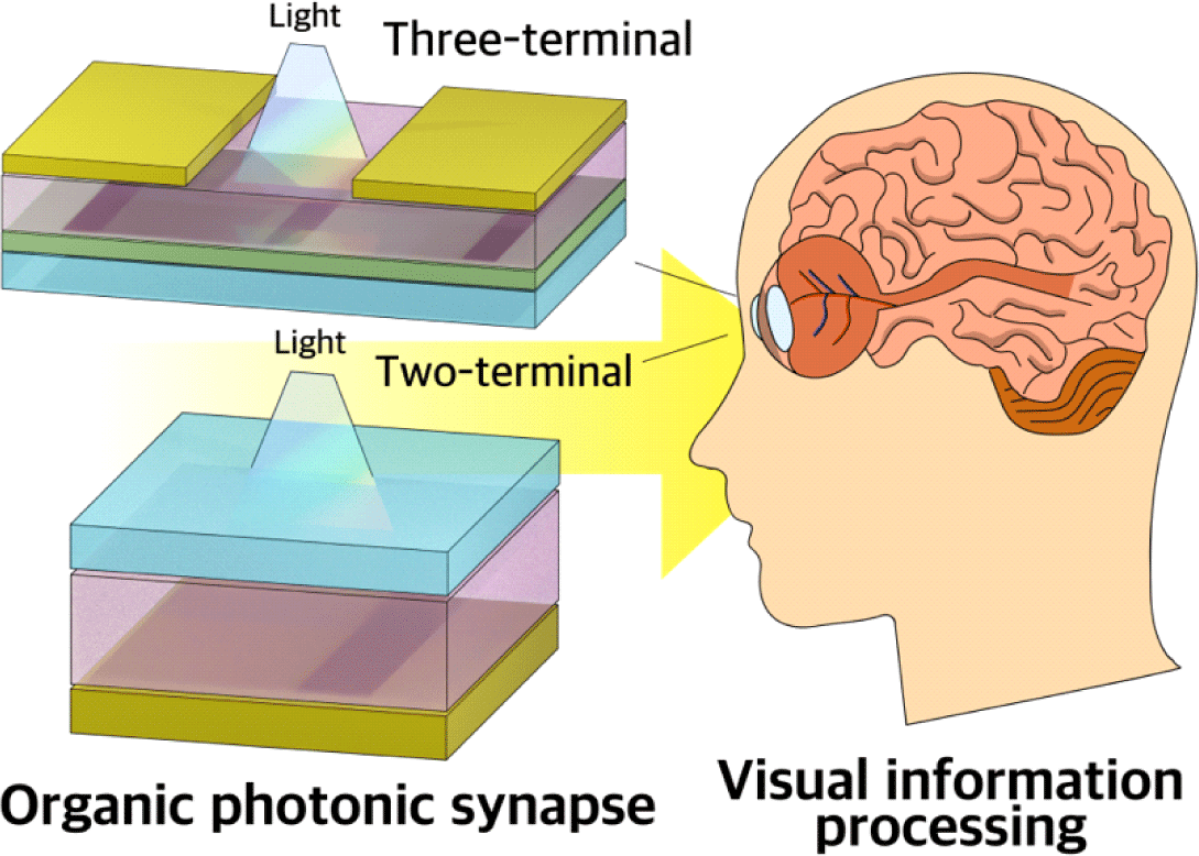
The realization of devices with synaptic properties and low power consumption is regarded as the basis for the implementation of neural networks and neuromorphic computation systems (Fig. 1). Recently, photonic synapses that exhibit various synaptic properties depending on the light exposure information (i.e., intensity, duration, and number) have attracted considerable attention owing to their high bandwidth, low energy consumption, and ultrahigh propagation speed [7-9]. Additionally, they enable wireless communication by providing a non-contact writing method [10]. To implement photonic synaptic devices, various materials have been applied, including metal oxides [11-16], low-dimensional materials [17-20], and perovskites [21-24]. In particular, organic materials have been proposed as suitable candidates for device fabrication because of their tunable properties according to the molecular design [25,26]. Moreover, they have the unique advantages of large-scale integration, mechanical flexibility, biocompatibility, and low-cost solution-processing techniques such as spin coating [27-29].
In this review, the recent progress in organic photonic synapses (OPSs) is comprehensively discussed. First, we introduce the basic knowledge of the functions of biological synapses. Then, photonic synapses are categorized in terms of device structure (two-terminal memristors and three-terminal transistors), and the operating mechanism is reviewed. Subsequently, advanced applications such as pattern recognition and smart systems are introduced. Finally, challenges for the future development of photo-neuromorphic computing are discussed.
2. BIOLOGICAL SYNAPTIC PROPERTIES
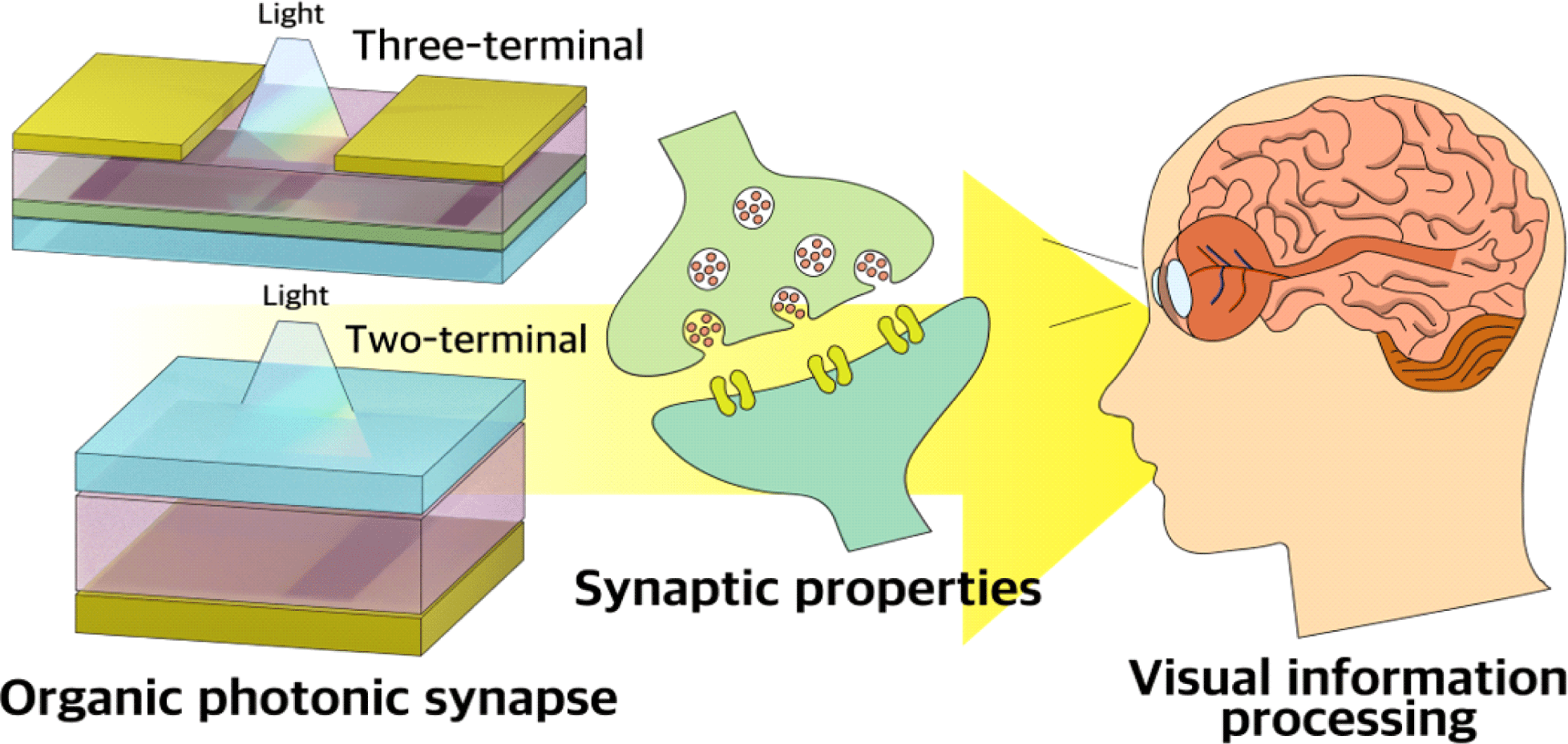
Synapses are the connection parts between the preneuron and postneuron [30]. Synapses are an important unit of learning and memory functions in the biological brain [31]. Therefore, the development of neuromorphic electronics that imitate biological synapses can be a solution to overcome the challenges of the current von Neumann computing process [32]. The synaptic properties should be replicated by neuromorphic devices. Synaptic plasticity can be mainly divided into short-term plasticity (STP) and long-term plasticity (LTP) [2,31]. When spikes are transmitted in the preneuron, neurotransmitters are released from the preneuron to the postneuron. These neurotransmitters instantaneously change the potential of the postneuron [34]. When the change in potential appears to be temporary, it refers to STP [31,35]. Paired-pulse facilitation (PPF) is caused by paired pulses; the postsynaptic potential induced by the second pulse is enhanced compared to the first postsynaptic potential. It can be represented as the paired-pulse ratio (PPR), which is the ratio of the second to the first postsynaptic potential [36-38].
The synaptic weight is adjusted according to the temporal interval between spikes [39,40]. This is called spike-timing dependent plasticity (STDP), which is one of the basic principles of Hebbian learning [41,42]. Spike rate-dependent plasticity (SRDP) indicates synaptic plasticity that is affected by the spike rate [43]. In addition, spike duration can change the synaptic weight; this is referred to as spike duration-dependent plasticity (SDDP) [44]. These repetitive and frequent stimuli lead to long-term changes in potential, indicating LTP.
3. MECHANISMS
Two-terminal artificial synapses mimic biological synaptic characteristics by changing the conductance (synaptic weight) of the active layer between two electrodes [44-48]. The active layer of two-terminal artificial synapse is equivalent to synaptic cleft of biological synapse, as the top electrode and bottom electrodes work as a preneuron and postneuron, respectively. When an external pulse corresponding to the action potential of a biological synapse is applied, conductance changes occur in the active layer. Recently, organic-based photonic memristors (OPMs) have been receiving research attention because they can exhibit the advantages of both organic materials and photonic devices, as aforementioned, in the aspect of a memristor.
OPMs realize synaptic responses mainly through the photogating effect. When an optical pulse is applied, the photogenerated carriers separated from excitons induced in the active layer are trapped at the interfacial defects between the electrode and active layer. This produces an additional electric field that can modulate the conductance of the active layer, which is called the photogating effect [49]. For instance, an OPM with an active layer of a photosensitive material, poly(3-hexylthiophene) (P3HT) [50], a top electrode of Au, and a bottom electrode of ITO is introduced. When the light is on, P3HT generates a number of excitons (electron–hole pairs). Then, the photogenerated excitons are separated and driven by the external electric field to overcome the interface barrier height, resulting in an increase in current. After the light is off, the trapped electrons at the interface of Au/P3HT are gradually released and recombined; the current is restored to its initial state showing a decay of current [51]. Likewise, an OPM consisting of a ReS2-Polyvinylalcohol (PVA) active layer, which is a photosensitive material exfoliated with PVA, successfully mimicked STP and LTP under photonic stimuli owing to the charge trapped in the shallow- and deep-level trap sites in the active layer, respectively [52].
In addition, an OPM with an additional ferroelectric layer using poly(vinylidene fluoride-trifluoroethylene) (P(VDF-TrFE)) was developed to control the relaxation behavior of the device. P(VDF-TrFE) was selected because it is a widely used ferroelectric material that has the advantages of low-cost solution processing, chemical stability, mechanical flexibility, and biocompatibility [53]. To induce the photogating effect, the device uses Copper(II) phthalocyanine (CuPc) as the active layer, which is a p-type semiconductor with electron trap states [54]. When the device is in the pristine state, the polarization of the ferroelectric layer is random, and there is no significant influence on the synaptic behavior of the device. However, when the ferroelectric layer is in the downward polarization state, the device shows a stronger photogating effect and longer relaxation of the excitatory postsynaptic current (EPSC) than that in the pristine state. The positive polarization charges at the P(VDF-TrFE)/CuPc interface induce a large energy well that interrupts the splitting of electrons to the ITO electrode. On the contrary, in the upward polarization state, the negative polarization charges at the P(VDF-TrFE)/CuPc interface accelerate the split of electrons to the ITO electrode, resulting in weaker photogating effect and shorter relaxation of the EPSC than that in the pristine state [55].
A photonic synapse transistor with three terminals (gate, source, and drain electrodes) mimics the function of a biological synapse by converting a presynaptic optical input into a postsynaptic electrical current output. Typical photo synaptic transistors mainly have the structure of a field-effect transistor (FET) and are composed of a gate electrode, dielectric, semiconductor, and source/drain electrodes. Under light stimulation, the excitons generated in the photosensitive material modulate the channel conductance (synaptic weight) between the source and drain electrodes. The channel conductance can also be controlled by the gate voltage. After the light is removed, the photoinduced charge carriers are recombined, and thus, the channel conductance returns to the original state. This increase and decay in the photocurrent is a source of various synaptic properties. In three-terminal (3-T) devices, the reading and writing paths are separated, and thus the transistors have the advantage of non-destructive readout operation. Transistor-based photonic synapses can be divided into two types according to their operating mechanisms: ferroelectric and charge trapping. In this section, recent studies on transistor-based photonic synapses are discussed based on their operating mechanisms.
Synaptic characteristics can be achieved through the polarization state of the ferroelectric material used as the gate insulator of the transistor [56-58]. By applying the input spike, dipole orientation of the ferroelectric gate insulator occurs, which changes the charge density of the channel, defined as synaptic weight. Ferroelectricity-based devices have the advantages of high operating speed and low power consumption owing to rapid electronic polarization by a low external electric field. Based on this mechanism, ferroelectric field-effect transistors using 2,7-dioctyl [1] benzothieno [3,2-b] [1]benzothiophene (C8-BTBT) and P (VDF-TrFE) as the channel and ferroelectric layers, respectively, have been reported [59]. Based on C8-BTBT’s excellent photosensitive properties and the stable ferroelectric polarization switching of P (VDF -TrFE), artificial synapses achieved extremely low energy consumption of 0.35 fJ, which is much lower than that of CMOS and biological synapses. The EPSC response and transition from short-term memory (STM) to long-term memory (LTM) were achieved in an organic ferroelectric synaptic device.
A hippocampal-synapse-mimetic system based on an organic synaptic transistor with a dual-gate geometry was demonstrated for the first time [60]. To improve the sensing stability, direct contact between the device and the buffer solution should be prevented. The dual-gate configuration enables stable detection of external stimuli by separating the dopamine-responsive electrodes. Furthermore, this structure effectively amplified the changes in the surface potential caused by dopamine stimulation. Based on an additional gate terminal and modulation of the remnant polarization of the ferroelectric top-gate dielectric (P(VDF-TrFE)), hippocampus-inspired artificial synapses showed synaptic operation by the simultaneous sensing of dopamine solution and light.
In this section, a photonic synapse based on the charge-trapping mechanism is introduced. The charge-trapping mechanism is classified into three types according to the trapping layer of the photoinduced electron–hole pairs (EHPs): floating gate, channel, and dielectric/OSC interface.
Compared to conventional FETs, floating gate (FG) transistors have a device configuration in which a photosensitive FG layer and dielectric layer are additionally embedded between the channel and gate insulator. For accurate conductance state updates, a dielectric layer with a large bandgap and low defect density is required as a tunneling layer to prevent charge-carrier recombination. Under light exposure, photoinduced charge carriers can be easily injected into the FG layer through the tunneling effect. Because the FG layer is completely blocked by the gate insulator and tunneling layer located at both ends, the trapped charge does not require an external gate voltage. Therefore, the nonvolatile channel conductance based on the stable maintenance of charge carriers makes FG-type transistors advantageous in mimicking LTM characteristics compared to other synaptic devices.
Strong photosensitive materials are usually involved in the construction of FGs to respond effectively to photostimulation. For photonic synapses that can modulate synaptic weights with UV stimulation, carbon nitride (C3N4) layers that strongly absorb UV light are used as FG layers [61]. A schematic of the device and microscopic morphology of the UV-responsive interfacial layer, characterized by scanning electron microscopy (SEM), are shown in Fig. 2(a). The operating mechanism of C3N4 based UV-responsive synaptic transistors (CNUVSs) is as follows. Under UV exposure with energy above the bandgap (Eg) of the photoactive FG, charge-carrier generation occurs in both the pentacene and NT-CN layers (Fig. 2(b)). Depending on the band alignment, photoinduced holes in NT-CN are injected into pentacene through the poly (methyl methacrylate) (PMMA) layer via the tunneling effect. The photoinduced electrons are trapped in the floating gate to form a negative potential for increasing IDS. When UV light is removed, the EHPs in pentacene immediately recombine, whereas electrons trapped in the NT-CN film have a long recombination time. This delay becomes a source of synaptic characteristics, and CNUVSs show various synaptic properties including PPF, SDDP, and SRDP.
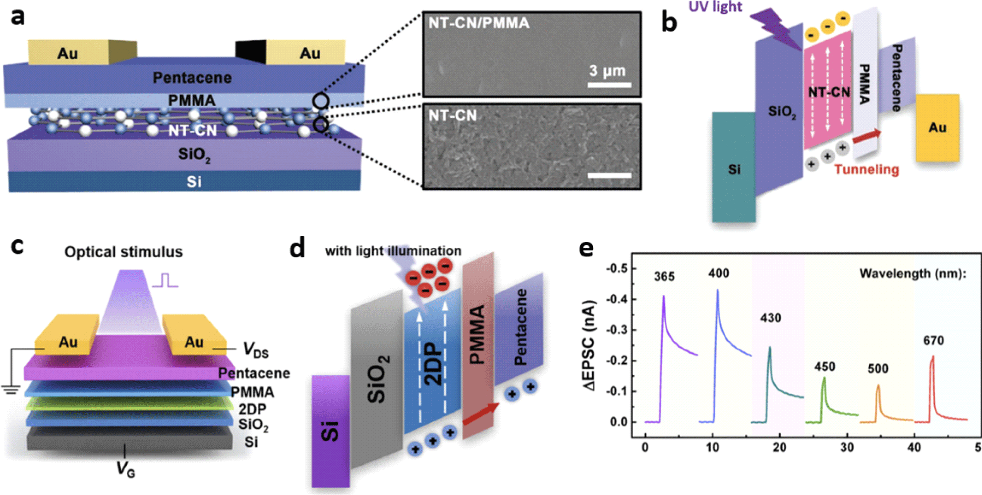
Photonic synaptic transistors based on two-dimensional polymers (2DPs) have been developed (Fig. 2(c)) [62]. Because the absorption bands of pentacene and 2DPs do not overlap, the transistor with a heterojunction structure of 2DP and the organic semiconductor exhibited a spectral-dependent synaptic response in the wavelength range of 365−670 nm. To explain the operation mechanism of the 2DP-based photonic synapse, an energy band diagram of the device under light stimulation is shown in Fig. 2(d). In this photonic synapse, several synaptic functions are mimicked, including EPSC, PPF, and transition from STM to LTM (Fig. 2(e)). Benefiting from the excellent absorption property of the 2DP, the device is driven with low operating voltage of −0.1 V, and ultralow power consumption of ∼0.29 pJ per synaptic event is thus achieved.
Transistors based on heterojunction channels of p-type and n-type organic semiconductors have been reported [63]. Under light stimulation, the energy level difference between the two semiconductors causes excitons to separate at the interface between the p-type and n-type semiconductors. This leads to more efficient charge separation in the channel; therefore, typical synaptic functions based on light stimulation are successfully modulated.
Artificial photonic synapses based on vertical organic field-effect transistors (VOFETs) have been developed for the first time [64]. Compared with conventional lateral transistors, VOFETs have the advantages of fast switching speed and low-voltage operation owing to their short channel length. In this vertical transistor, single-walled carbon nanotubes and PEDOT: PSS are used as the source and transparent drain, respectively. Poly [2,5-bis (2-octyldodecyl)pyrrolo [3,4-c] pyrrole-1,4 (2H,5H)-dione-3,6-diyl)-alt-(2,2′;5′,2″;5‴, 2‴-quaterthiophen-5,5‴-diyl)] (PDPP4T) was adopted as a channel material and CsPbBr3 quantum dots as a light-harvesting material. The charge-carrier generation and transport between CsPbBr3 and PDPP4T are as follows. Under light illumination, the photogenerated holes in CsPbBr3 quantum dots are immediately transferred to PDPP4T, whereas the photogenerated electrons remain in CsPbBr3. When the light is off, the holes injected into the PDPP4T layer slowly recombine with electrons because of the large energy barrier between the valence band of CsPbBr3 and the highest occupied molecular orbital (HOMO) of PDPP4T. The slow recombination of charge carriers leads to slow photocurrent recovery. A study of lateral transistors using CsPbBr3 quantum dots channels has also been reported [65]. Based on the mechanism described above, important synaptic properties, such as EPSC, PPF, and STP-to-LTM conversion, were mimicked.
A 2D perovskite/organic heterojunction (PEA2SnI4/ Y6) ambipolar synapse phototransistor with near-infrared (NIR) wavelength selectivity was demonstrated [66]. The absorption spectrum of PEA2SnI4/Y6 is over the visible light and NIR light range, and photodetection is possible over a wide absorption wavelength range of 300−1,000 nm. When the device is irradiated with visible light, EHPs are generated in both perovskite and Y6. The photogenerated electrons are captured by defects (Sn vacancies) in the perovskite layer, which cause a strong photogating effect. When the device is irradiated by NIR light, the photogenerated holes in Y6 are transferred to the perovskite and trapped at the interface of PEA2SnI4/Y6, increasing the photocurrent. Furthermore, a transistor with the same mechanism based on a C8-BTBT/copper hexadecafluorophthalocyanine (F16CuPc) heterojunction channel has been reported [67]. The plasticity of this synaptic device can be modulated using broadband light sources, including near-ultraviolet (NUV), visible, and NIR light sources.
Photonic synapses based on organic molecular crystals (OMCs) have been demonstrated [68]. For device fabrication, 5,11-bis (triethylsilylethynyl) anthradithiophene (Dif-TES-ADT) has been used as the photoactive layer owing to its broad light absorption band
and high charge mobility. Crystals with fewer defects enhance charge transport and accelerate exciton extraction. Divinyltetramethyldisiloxane-bis (benzocyclobutene) (BCB) and SiO2 were used as dielectric layers. Under light irradiation, the photoinduced electrons generated in Dif-TES-ADT are transferred to oxygen-related levels, and O2− anions are formed. The photoinduced holes move to the BCB/ Dif-TES-ADT crystal interface. Exposure to stronger light increases the EHPs produced in the active layer, leading to the formation of more O2− anions. A high concentration of O2− anions creates an oxygen-related trap inside OMCs. As a result, the anions remain stable over a long lifetime. These negative charges induce a gate effect, which leads to a continuous hole injection and maintains a highly conductive current state.
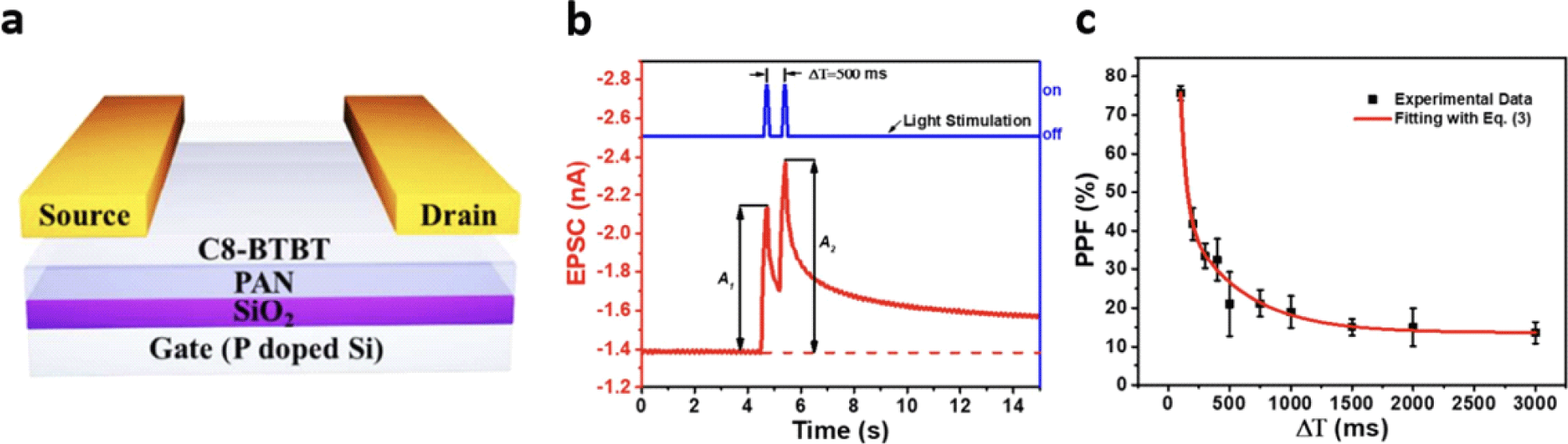
The interfacial charge-trapping effect between dielectrics and semiconductors is widely used as an effective strategy to implement photosynaptic transistors. Many studies using various organic small molecules, including C8-BTBT [69,70,73] and pentacene [62,71, 74-77], have been reported. Owing to the high mobility and stability of C8-BTBT, a photonic synapse using C8-BTBT as a channel and a polyacrylonitrile (PAN) film as a dielectric layer has been demonstrated (Fig. 3(a)) [69]. The excitons generated under UV light are separated by the electric field, and the photoinduced electrons are trapped at the C8-BTBT/PAN interface. The polar groups of PAN enhance the trapping effect at the interface by providing charge trap sites. When the stimulus is removed, the trapped charges are released, leading to decay of the EPSC. Fig. 3(b) and Fig. 3(c) show the basic synaptic functions realized in the device. Based on a similar operating principle, C8-BTBT OFETs that show an effective OSC/dielectric interface through octadecyltrichlorosilane surface modification have also been reported [70]. As regards pentacene, the charge-trapping dynamics of poly(2-vinyl naphthalene) (PVN)/pentacene interfaces have been studied [71].
To control the exciton dynamics at the interface, the tunneling effect-assisted charge-trapping concept has been studied [72]. By inserting an additional tunneling barrier layer between the active layer and dielectric layer, the photoinduced charges can be stably trapped. The working principle of the device using the tunneling effect is as follows. During the photowriting process, the excitons generated in the channel are dissociated, the holes remain in the channel, and the electrons penetrate the tunneling layer and are trapped at the interface of the dielectric layer. Subsequently, during the recovery process, in which the applied light stimulus is removed, the remaining holes in the channel pass through the tunneling layer and recombine with electrons so that the device returns to the OFF state.
4. APPLICATIONS
As various materials and structures of OPSs have been investigated, researchers have attempted to use OPSs in actual applications. One of the goals of neuromorphic electronics is hardware implementation to emulate the abilities of the biological brain, which enables learning, memorizing, and recognizing data with low energy consumption and parallel processing. In this chapter, practical applications such as pattern recognition, Pavlovian conditioning, and smart window were introduced for future neuromorphic systems.
Neuromorphic optoelectronics exhibit potential for biomimetic applications that can learn, memorize, and recognize visual information. Thus, photonic artificial neural networks (ANNs) that emulate the preprocessing of visual perception have been studied, such as pattern and image recognition [78]. These ANNs update the synaptic weights by applying training algorithms for forward and backward propagation [79]. under illumination. The learning procedure of the ANN is mainly divided into two parts. During forward propagation, input data (x) from the neurons are weighted with each value (synaptic weight, w) and transmitted to the other artificial neurons. Then, outputs (y) emerge from the added inputs. After forward propagation, the synaptic weight is modulated using a supervised learning method that updates the weight through backpropagation to adjust the error between the output and target values [80]. In addition, the handwritten digit pattern from the Modified National Institute of Standards and Technology (MNIST) database is widely used for training and testing for image processing systems.
To enhance the accuracy of pattern recognition, the devices should have multiple controllable conductance states, as well as stable and linear potentiation/depression by continuous light pulses. An ANN that used OPSs based on CuPc/p-6P achieved a maximum recognition rate of 78% owing to its excellent LTP characteristics. This accuracy value is high when considering that this ANN system uses a single-layer network and a unidirectional update method [81]. Moreover, an ANN consisting of OPSs with an additional ferroelectric layer (P(VDF-TrFE)) significantly improved the accuracy, achieving 90.6%, for recognizing digits in the MNIST database. The LTP/LTD properties of this device were enhanced owing to the stable ferroelectric polarization switching of P(VDF-TrFE) [59].
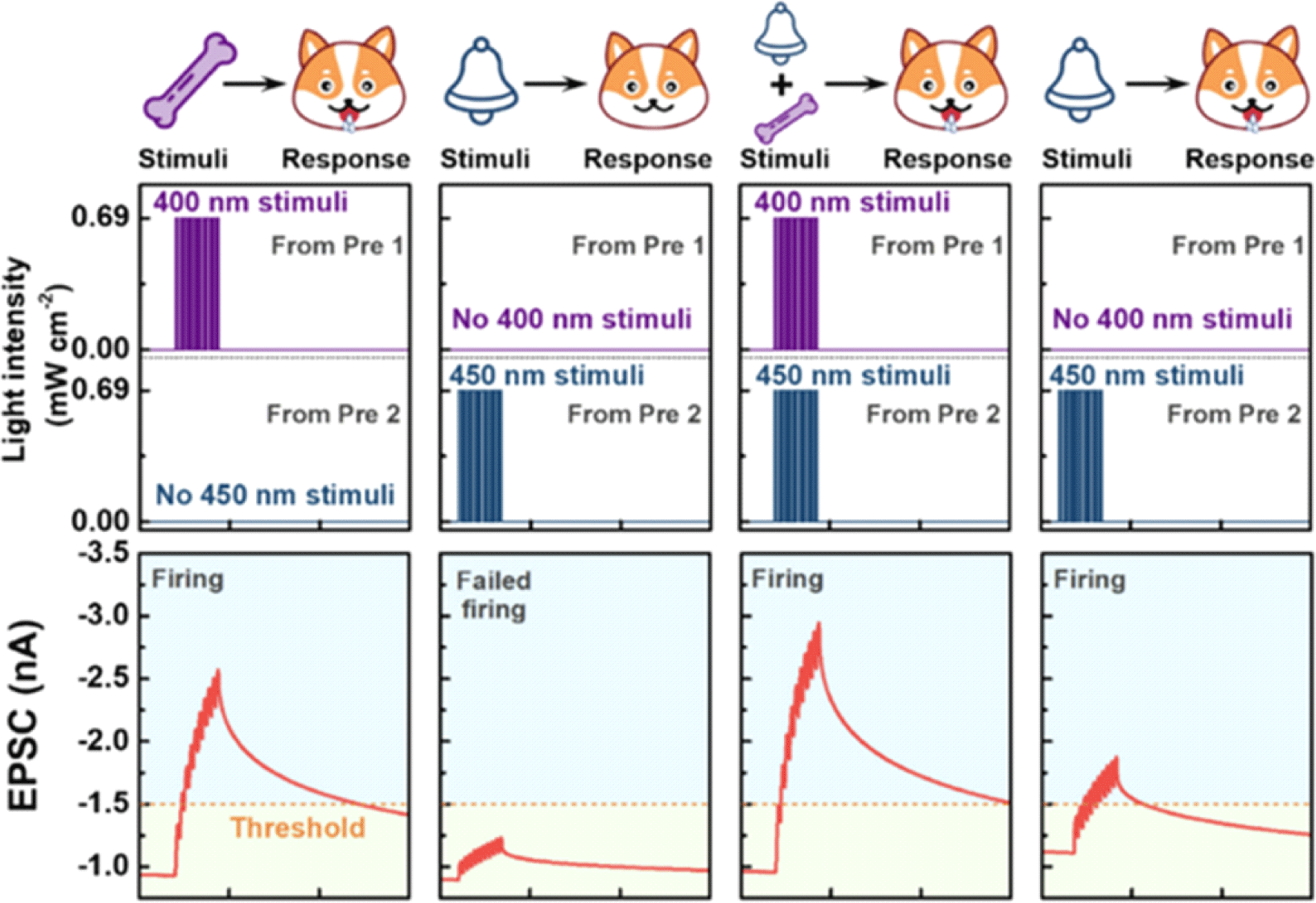
Pavlov’s dog experiment (also called the classical conditioning experiment) using photonic synapses was performed to mimic the associative learning process that occurs in the human brain. Classical conditioning is the induction of a neutral stimulus into a conditioned stimulus (CS) by repeatedly associating a neutral stimulus with an unconditioned stimulus (US), and this change in behavior through experience is called learning. Association learning was performed using Pavlov’s dog experiment with a spectrum-dependent photonic synapse [62]. 2D polymers with high photosensitivity were used as the photoactive charge-trapping layers. Light stimulation with a wavelength of 400 nm corresponds to food, that is, unconditioned stimuli, and light with a wavelength of 450 nm corresponds to bell ringing (conditioned stimuli). It is defined as a salivation response when the EPSC value is higher than the threshold (EPSC=−1.5 nA). Before the association condition was established, only food stimulation with 400 nm light exposure caused a salivation response (Fig. 4). The bell ringing stimuli (450 nm light exposure) showed EPSC values lower than the threshold for salivation, indicating no response. Bell ringing and food stimuli were simultaneously applied during training to establish an association between bell ringing and salivation response. Subsequently, the association between the bell and the salivation response was established; ringing the bell without food can show salivation behavior of EPSC values greater than the threshold current. This means that food and ringing were successfully linked, and the ringing of the bell became a CS.
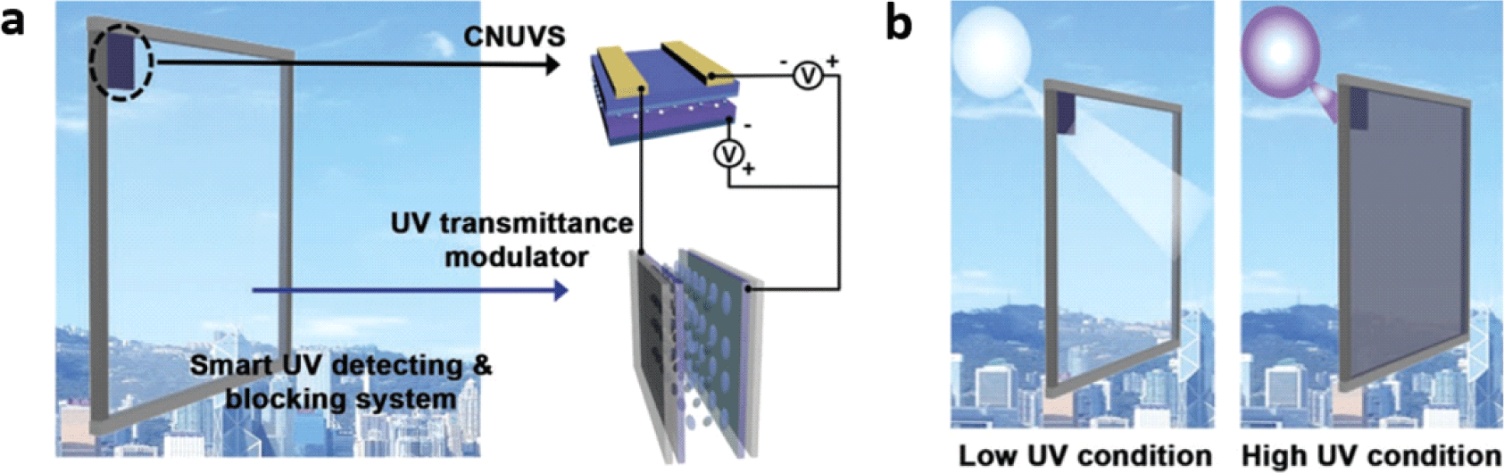
It is important to emulate the visual perception of the retina, as more than 80% of the information acquired from external stimuli depends on the visual sense. To mimic the visual sense, a retina-inspired organic photonic synapse using C3N4 nanodots as a UV-responsive FG layer was developed [61]. UV radiation, which causes skin aging, skin cancer, and cataracts, is harmful, but the human retina cannot detect it. A smart system that detects and blocks UV light was demonstrated by integrating a transmittance modulator and a UV-responsive synaptic transistor (Fig. 5(a)). Photonic synapses, which contain the dual functions of artificial synapses and photosensors, can detect and process UV exposure information (optical signals), including light intensity, number of exposures, duration, and frequency. Therefore, the smart window system can monitor UV dosage according to the duration of UV exposure. As shown in Fig. 5(b), UV-induced diseases can be prevented in advance by controlling the transmittance of UV rays through a window during UV exposure. Furthermore, UV-responsive photonic synapses can extend the human visual sense beyond visible light, and this could be applied to other healthcare devices such as smart glasses or artificial retinas for soft humanoid robots.
5. PERSPECTIVE AND FUTURE PROSPECTS
We reviewed OPSs that have the advantages of organic materials and optical signals. Compared to inorganic materials, organic materials are promising candidates owing to their unique advantages of low cost, large-scale integration, flexibility, biocompatibility, and tunable properties according to molecular design. At the same time, compared with electrical synapses, photonic synapses have the advantages of wide bandwidth, low energy consumption, and ultrahigh propagation speed. As most OPSs consist of light-sensitive active layers, it is possible to express the synaptic properties of biological synapses by converting optical signals into electrical signals. Therefore, we explain the biological synaptic behaviors and operating mechanisms of OPSs to exhibit these synaptic properties. Two-terminal devices mostly show synaptic properties with a photogating effect induced by trapped charges in the interfacial defects, whereas three-terminal devices show synaptic properties with ferroelectricity and charge-trapping/detrapping mechanisms. Applications using OPSs have been researched to mimic human vision, such as pattern recognition and smart windows that can detect UV rays beyond the human retina range. In the future, these applications could be applied to artificial retinas for soft humanoid robots, or even to replace human retinas. In addition, classical conditioning experiments, such as Pavlovian conditioning, have also been conducted to mimic the associative learning process of the human brain.
Although various photosensitive materials and device designs have been developed to create OPSs, progress is needed in this area. First, synaptic depression of the devices was achieved by electrical pulses, whereas potentiation behavior was achieved by photonic stimuli. Hence, not only through materials that are inherently photo-responsive, but innovative architectures that could achieve both potentiation and depression behavior by light are also needed to develop genuine optical wireless communication devices. Lastly, photonic devices still suffer from nonlinearity, performing far less accurately in image or pattern recognition compared to electrical synapses. Therefore, finding optimal materials and device structures for OPSs will address the challenges mentioned above, and could be a breakthrough for future synaptic devices in biomimetic synapses and neuromorphic computing.