1. INTRODUCTION
Colloidal quantum-dot (QD) light-emitting diodes (QLEDs) have been considered as one of the promising candidates due to their excellent optoelectronic properties, such as size-dependent tunable bandgap, wide absorption, and high color purity with near-unity photoluminescence quantum yield (PL QY) [1-4]. In particular, the demand for flexible QLED displays as informative optoelectronic devices has significantly increased due to their high free-form factor, which is necessary in cutting-edge displays such as augmented/virtual reality, wearable glasses, and foldable/rollable smartphones that must be thin, light, flexible, and bendable [5-7]. This is because convenient and secure contact without the feeling of irritation is crucial for the comfort of the user in daily life. In this sense, portable lighting and display devices that can be user-interactive and freely available in the deformable shape is indispensable in human-lives [8-9].
There have been several advances in the development of wearable QLED displays that can be fabricated on flexible substrates. In 2015, Choi et al. reported the deformable and ultra-thin QLEDs display on curved and convoluted surfaces [10]. In 2020, Shin et al. reported waterproof and flexible InP based QLEDs on polyethylene naphthalate (PEN) substrate using CYTOP encapsulation layer [11]. In 2021, Kim et al. also reported 3-dimensional foldable QLEDs on a Parylene C that can be created using laser patterning and metal etch-stop layers with customized ablation thresholds [12]. Despite these achievements, however, most of the papers have focused on the fabrication method capable of making the devices thin, light, waterproof, and skin attachable. However, for QLEDs that remain highly luminous and stable even under curved and deformable shapes, the low thermal conductivity (κ) values (<0.3 W/m·K) of conventional flexible substrates should be improved. Because of the low κ of the substrate, the light-emitting pixels in operation may experience thermal degradation at high current densities (J) due to Joule heating. To resolve this challenge, several attempts have been made by the adoption of high-κ substrates such as sapphire, Si, and Al-metal foil substrate, showing 46 W/m·K, 150 W/m·K, and 237 W/m·K, respectively [13-15]. However, these works have been attempted on inflexible substrates or on metal foils, so the stable operation of QLEDs is vulnerable to the repeatable deformable stress.
In this study, we have demonstrated bright and efficient QLEDs in an inverted top-emitting structure, which are fabricated on a PEN substrate with a thin (200 nm) Al-based heat dissipation layer. As a result of the enhanced heat dissipation property, the flexible top-emitting QLED (TQLED) exhibited a high luminance (L) of ∼366,000 cd/m2 and high current efficiency (CE) of 43.3 cd/A, while it stably operated at a high J up to 2,300 mA/cm2. Furthermore, we adopted Parylene C and SU-8 for both surface planarization and device encapsulation, making the flexible device waterproof. We posit that our approach to device design for developing flexible, wearable QLED displays provides valuable insights.
2. METHODS
The CdSe/Cd1−xZnxS QDs were synthesized in the same method reported previously [9]. To prepare the ZnO nanoparticles, first, 80 mL of methanol and 2 g of zinc acetate dehydrate (Zn(CH3COO)2η2H2O) were mixed in a three neck flask. When the temperature grew up to 60°C in N2 atmosphere, potassium hydroxide dissolved in methanol (23.25 mg mL−1) was added into the flask at the rate of 238.5 mL h−1. After 150 min of reaction, the ZnO nanoparticles were sunk down for 12 h. After that, the solution was centrifuged at 4,000 rpm for 3 min to extract pure ZnO nanoparticles from the mixture solution. Finally, the ZnO nanoparticles were redispersed in 1-butanol.
To confirm the performance of the thin heat dissipation layer, we prepared the TQLED either on a typical PEN substrate or on the Al-coated PEN substrate. A 2.0-μm-thick Parylene C layer was deposited using a Parylene deposition system (PDS 2010). After that, a 500-nm-thick epoxy (SU-8 2000.5, MicroChem) layer was spin-coated on the Parylene C layer for planarization for both substrates. On the substrates, a 100-nm-thick Ag layer was deposited as the reflective cathode electrodes by thermal evaporation. Then, the ZnO nanoparticles (20 mg/mL) were spin-coated at a rate of 2,000 rpm for 40 s, followed by annealing at 100°C for 30 min. The red-emitting CdSe/Cd1-xZnxS QDs (20 mg/mL in toluene) were deposited by spin-coating at a rate of 4,000 rpm for 30 s, and then dried at 90°C for 30 min. Then, 4,4’-bis (9-carbazolyl)-biphenyl) (CBP, 50 nm), MoOx (5 nm), dipyrazino[2,3-f:2’,3’-h] quinoxaline-2,3,6,7,10,11-hexacarbonitrile (HAT-CN, 5 nm) and Ag (20 nm) were sequentially deposited by thermal evaporation as the hole transport layer, the hole injection layer, and the anode, respectively.
The transmission electron microscopy (TEM) image was obtained using a Cs-corrected TEM (JEOL JEM-ARM200F). The surface morphology of the flexible substrates was obtained using an atomic force microscopy (AFM) (Park Systems NX-10). The J–voltage (V)–L characteristics of the TQLEDs were measured using a Keithley 236 source–measure unit, a Keithley 2,000 multimeter, and a calibrated Si photodiode (Hamamatsu, S5227-1010BQ). The electroluminescence (EL) spectra were measured using a spectroradiometer (Konica–Minolta CS-2000). For the thermal simulations, a COMSOL Multiphysics software was used.
3. RESULTS AND DISCUSSION
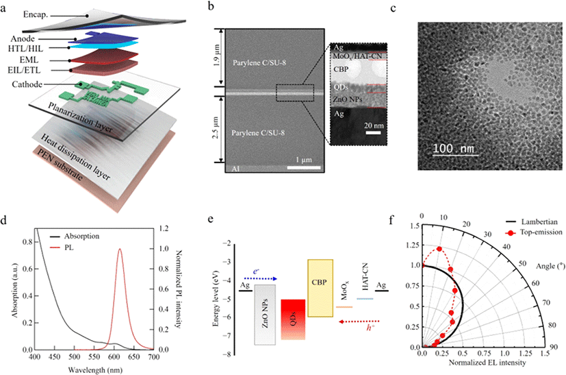
Fig. 1(a) shows an exploded view of the flexible TQLED while Fig. 1(b) presents the cross-sectional TEM images of the TQLED device. We deposited a thin (200 nm) Al layer on the flexible PEN substrate as a heat dissipation layer. To alleviate the surface roughness of the substrate, Parylene C and SU-8 layers were deposited, because of their low temperature processability and high flexibility, in comparison to inorganic planarization/passivation layers, such as SiO2, Si3N4, and HfOx [16-17]. For the TQLEDs, we utilized red CdSe/Cd1−xZnxS QDs as the emissive layer (EML), of which an average diameter is 13.2±1.2 nm, as shown in Fig. 1(c). Fig. 1(d) shows their PL and absorption spectra; a PL peak wavelength at 614 nm, a full-width at half-maximum of 31 nm, and a PL QY of 80%. As shown in Fig. 1(b) and 1(e), the TQLED consist of Ag (85 nm)/ZnO nanoparticles (40 nm)/QDs (20 nm)/CBP (50 nm)/MoOx (5 nm)/HAT-CN (5 nm)/Ag (20 nm). For the efficient hole injection, we adopted MoOx/HAT-CN as a hole injection layer, as reported previously [14]. On the top of the device, the Parylene C/SU-8 bilayer was formed again for the water-resistant and ultra-thin encapsulation. Furthermore, to record the angular distribution of TQLEDs, we measured EL intensity along with the light-emission angle degrees from 0° to 90°. Fig. 1(f) shows that the TQLED emits light more to the normal direction deviating from the Lambertian profile, which is attributed to the microcavity effect between two reflective metal electrodes [18]. For comparison, we also prepared the same device on a normal PEN substrate, and analyzed their surface roughness, heat dissipation properties, and TQLED device performance.
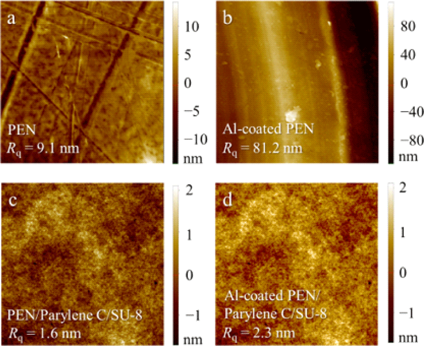
For bright and efficient flexible QLEDs, uniform surface morphology of flexible substrates is essential [19]. As shown in the AFM images in Fig. 2(a) and 2(b), the root-mean-square surface roughness (Rq) values of the PEN and the Al-coated PEN substrates were measured to be 9.1 nm and 81.2 nm, respectively. Also, the peak-to-valley values were high as several tens of nanometers for both cases. For the surface planarization of the substrates, a bilayer consisting of Parylene C/SU-8 was adopted, leading to uniform surface roughness with the Rq values of ∼2 nm for the two substrates, as shown in Fig. 2(c) and 2(d).
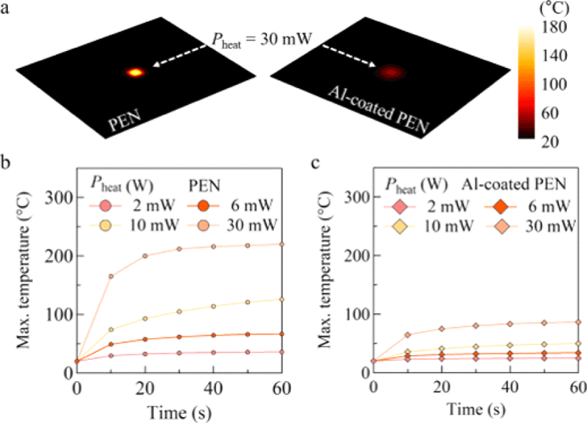
Next, we characterized the heat dissipation properties of the substrates. It is known that general polymeric materials have low κ values; for instance, κ of PEN, Parylene C, and SU-8 are ∼0.19 W/m·K, 0.08 W/m·K, and 0.2 W/m·K, respectively [20-22]. Thus, if Joule heat is generated during device operation, it impedes heat dissipation and can cause device degradation. However, by inserting a thin Al-based heat dissipation layer into the substrate, Joule heat can be effectively dissipated to prevent device degradation owing to the high κ of Al (237 W/m·K). In order to clarify the influence of the thin Al layer, placed between the PEN substrate and the Parylene C/SU-8 planarization layer, on the heat dissipation, we conducted thermal simulations using a COMSOL Multiphysics software. In this simulation, heat radiation and air-cooling were ignored. Fig. 3(a) shows the simulated temperature profile of the pixels on the respective substrate, where the pixel was considered as a Joule heat source with the applied power (Pheat) of 30 mW. For the accuracy of Pheat, the optical output power should be subtracted from the applied electrical power (i.e., current × voltage). However, since the optical power is negligible when compared to the electrical power, we simply assumed that Pheat is identical to electrical power [23]. The pixel with a dimension of 1.4 mm × 1.4 mm were positioned at the center of the substrate with an area of 20 mm × 24 mm, which are identical to the devices. The simulation results of the maximum pixel temperature with varying Pheat on the PEN and Al-coated PEN substrates are plotted in Fig. 3(b) and 3(c), respectively. It is obvious that the temperature on the Al-coated PEN substrate is much lower than that in the normal PEN substrate. For example, when Pheat is 30 mW, the pixel temperature on the PEN substrate was increased over 200°C which is high temperature sufficient to deteriorate the TQLED [13,24-25]. Meanwhile, the maximum temperature of the pixel on the heat dissipation layer-coated PEN substrate reached below 100°C at the same condition, verifying the heat dissipation ability of the thin Al layer. Therefore, it is expected that the TQLED fabricated on the Al-coated substrate can endure much higher current densities than that prepared on the normal PEN substrate.
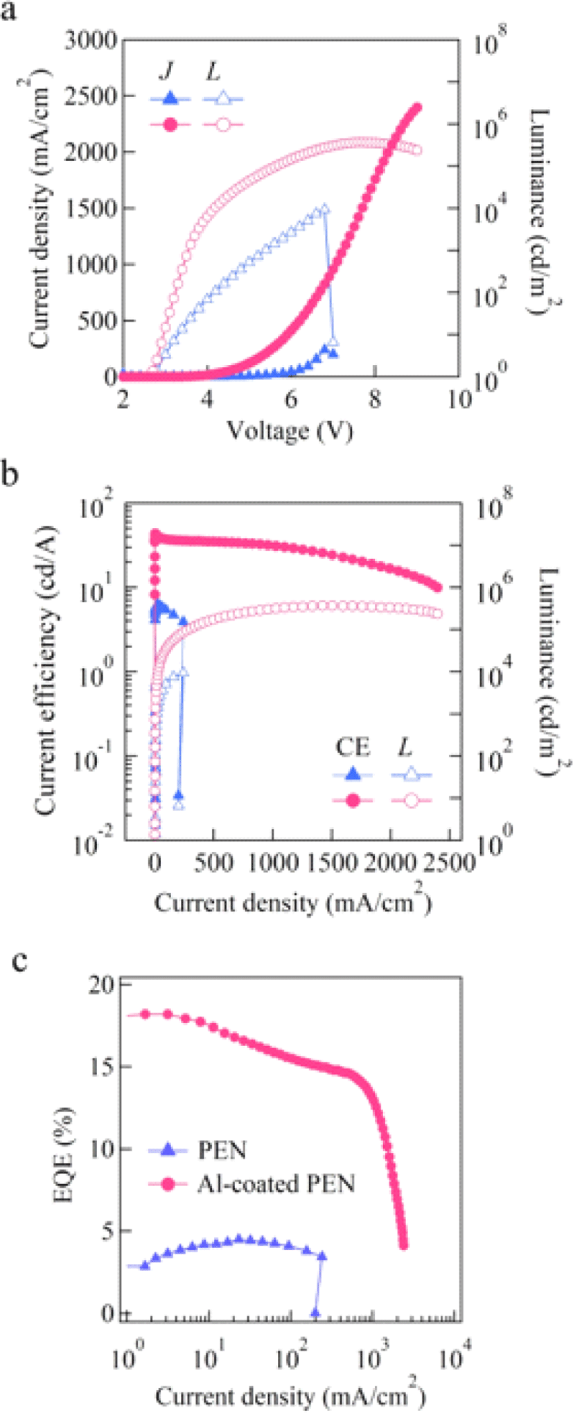
To confirm this, we measured the device performance of the TQLEDs fabricated on the PEN and Al-coated PEN substrates. As shown in Fig. 4(a), the TQLED on a normal PEN substrate presents catastrophic failure at J of ∼240 mA/cm2 at 6.8 V, which corresponds to ∼30 mW of Pheat. Since the simulation showed that 30 mW of Pheat can result in a pixel temperature >200°C, the failure is attributed to the Joule heat. On the other hand, the TQLED fabricated on the substrate with the heat dissipation layer could endure much higher J of up to 2,300 mA/cm2 (9 V), which generates Pheat of >400 mW. Furthermore, CE, the maximum L (Lmax), and external quantum efficiency (EQE) were significantly improved from 6.2 cd/A, 9,420 cd/m2, and 4.51% to 43.3 cd/A, 366,000 cd/m2, and 18.19%, respectively, as shown in Fig. 4(b). These results clearly show that the insertion of the thin metal-based heat dissipation layer is an excellent strategy to improve the performance of flexible QLEDs based on any types of plastic substrates, such as poly(ethylene-terephthalate) (PET), polyethersulfhone, and polyimide. The device performance of a few flexible QLEDs are compared in Table 1.
| Substrate | EL peak (nm) | Lmax (cd/m2) | CE (cd/A) |
|---|---|---|---|
| Parylene C/SU-8 [26] | ~540 | 44,700 | 4.5 |
| Parylene C/SU-8 [12] | ~550 | 50,500 | - |
| PET [27] | 606 | 106,890 | 16.3 |
| Al foil [5] | 624 | 39,880 | 3.6 |
| PEN (this work) | 9,420 | 6.2 | |
| Al-coated PEN (this work) | 621 | 366,000 | 43.3 |
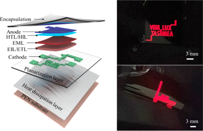
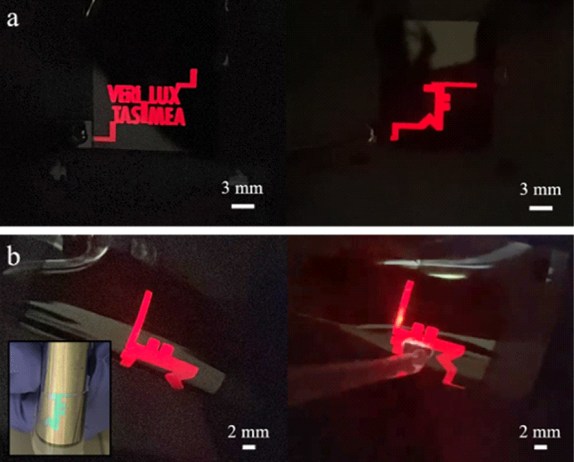
In addition to the improved device performance of the TQLEDs, we demonstrate the waterproof property which is indispensable for wearable application. We fabricated the devices with larger emission patterns on the substrates with a dimension of 30 mm × 40 mm. As displayed in Fig. 5, the letters and symbol patterns on the device stably emit red light while curled up in the pen. Additionally, owing to the Parylene C/SU-8 passivation layer, the device shines well even with a water droplet. Based on these results, we believe that our strategies for bright and efficient flexible QLEDs would be helpful for the development of human interactive display in near future.
4. CONCLUSION
In conclusion, we have demonstrated highly bright, efficient, and water-resistive flexible TQLEDs that hold promise for a range of applications. To address the low-κ of typical plastic-based flexible substrates, we developed a PEN substrate with a thin metal heat dissipation layer to improve the heat dissipation property. As a result, our TQLEDs exhibited significantly higher brightness and current efficiency compared to previously reported flexible QLEDs. Furthermore, we have successfully showed the large-area devices that can operate even in wet conditions, meeting the necessary requirements for flexible and wearable displays. We believe that our methodology will provide helpful insight and contribute to the development of wearable optoelectronic devices.


