PDF Download
 PubReader
 Export Citation
 Email the Author
 Share Facebook
 Share Twitter
 Cited by 0 Article
 Metrics (View:2,719)






1. INTRODUCTION
Organic optoelectronic devices–including organic light-emitting diodes (OLEDs) [1,2], organic photovoltaics (OPVs) [3,4], and organic photodetectors [5,6]– have attracted considerable attention due to their mechanical flexibility, low weight, and compatibility with cost-effective large-area fabrication. Among these technologies, OLEDs have achieved rapid commercial success in display applications, and are being actively explored for flexible and stretchable electronics [8,9], driven by advantages such as high efficiency, deep-black expressions, wide color gamut, and fast response times [10].
OLEDs consist of multiple organic thin films stacked between an anode and a cathode, where injected electrons and holes recombine in the emissive layer to generate light. To probe charge and exciton dynamics in these multilayer devices, capacitance-based analysis has been widely employed [11–13]. The capacitance, defined as C=dQ/dV, quantifies how the stored charge Q responds to a small voltage perturbation dV around a given bias V [31]. Because individual charge processes occur on distinct voltage and frequency scales, the voltage- and frequency-dependent capacitance measurements provide rich information on charge storage, transport, recombination, release, and ultimately device degradation.
From a structure perspective, an OLED can be viewed as a vertically stacked metal–insulator–metal system, in which organic layers with low free-carrier density serve as the dielectric. In the absence of carrier injection, the device exhibits a geometric capacitance Cgeo =ɛA/d, determined by the permittivity ɛ, device area A, and total organic thickness d. Under forward bias, however, injected carriers redistribute within the device, causing the measured capacitance to deviate from Cgeo.
The bias- and frequency-dependent capacitance modulation is mainly governed by two factors. The first arises from charges trapped in localized states within the bulk or at interfaces [14–18]. Because trapping and detrapping occur on relatively slow timescales, trap occupancy can follow a small-signal voltage modulation at low frequencies (typically below ~102 Hz), contributing directly to dQ/dV. The second contribution originates from charge accumulation at metal–organic or organic–organic interfaces when carrier injection is limited by energy barriers or mobility imbalance [19,20]. The resulting space-charge modifies the internal electrical field and hence the capacitance. Consequently, the capacitance becomes highly sensitive to injection barriers, carrier mobilities [13,21], trap distributions [22–24], and interfacial energy-level alignment [12,25,6].
Among capacitance-related phenomena, negative capacitance (NC) has attracted particular attention [29,30]. NC refers to an inductive-like small-signal response in which the capacitance becomes negative. As illustrated in Fig. 1, NC can appear in capacitance–voltage (C–V) characteristics at sufficiently high forward bias (Fig. 1(a)), or in capacitance–frequency (C–f) characteristics at low frequencies under a fixed bias (Fig. 1(b)). Because the geometric capacitance (Cgeo) is intrinsically positive, the emergence of NC represents an anomalous response that reflects complex, non-equilibrium charge dynamics within the device. Accordingly, NC has been extensively investigated both experimentally [20,27-29] and theoretically [19,30].
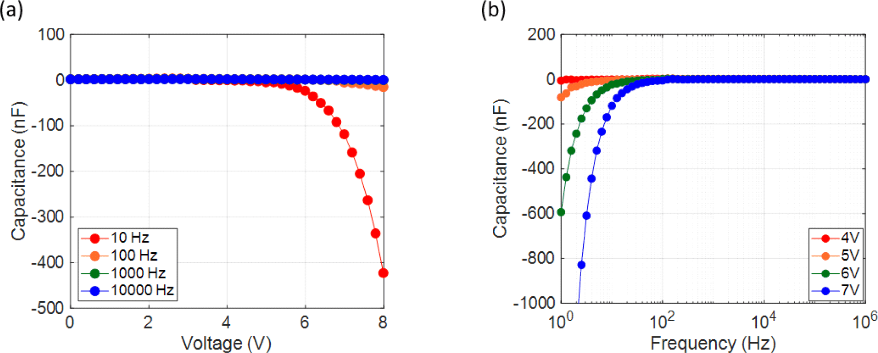
NC was first reported in inorganic semiconductor devices, including Si and GaAs diodes, Schottky junctions, metal–insulator–semiconductor structures, and multi-quantum-well detectors [7,39]. Although early studies often attributed NC to measurement artifacts, subsequent work established it as a genuine physical signature of imbalanced charge dynamics. Later impedance spectroscopy studies demonstrated that NC also occurs in organic semiconductor devices [22,29,32,33], indicating that it is a general phenomenon not restricted to inorganic systems. In OLEDs, NC is now widely regarded as a sensitive indicator of charge processes such as injection, recombination, trapping, and interfacial accumulation [19,22,32].
Despite this progress, the microscopic origin of NC remains controversial. Many studies attribute NC to bipolar carrier injection and recombination [19,22,28, 29,32,34], whereas other experimental and simulation results show that NC or inductive-like responses can also be found under unipolar operation [30,35]. This discrepancy complicates the identification of the dominant mechanisms responsible for NC. To address these issues, this review first discusses how NC manifests in various capacitance measurements (Section 2), then overviews experimental observations and proposed mechanisms, including bipolar recombination (Section 3.1), injection imbalance (Section 3.2), interfacial charge accumulation (Section 3.3), energetic disorder (Section 3.4), and self-heating (Section 3.5). Through this discussion, we aim to clarify the conditions under which NC emerges and what aspects of internal charge dynamics it reflects.
2. THEORETICAL AND EXPERIMENTAL METHODOLOGY
Impedance spectroscopy is a fundamental technique for quantitatively analyzing charge dynamics in OLEDs [11,36,7], including the emergence of NC. In a typical measurement, a small sinusoidal voltage, Ṽ(ω)=Vdc+V0 cos(ωt), is applied to the device, where Vdc is the dc bias, V0 is the small-signal amplitude, and ω is the angular frequency. The resulting current response Ĩ(ω) is measured simultaneously, as schematically illustrated in Fig. 2(a). Although Ĩ(ω) oscillates at the same frequency ω, its amplitude and phase generally differ from those of Ṽ(ω) due to the device’s resistive and reactive components. The impedance Z(ω), or the inverse of the admittance Y(ω), is given by:
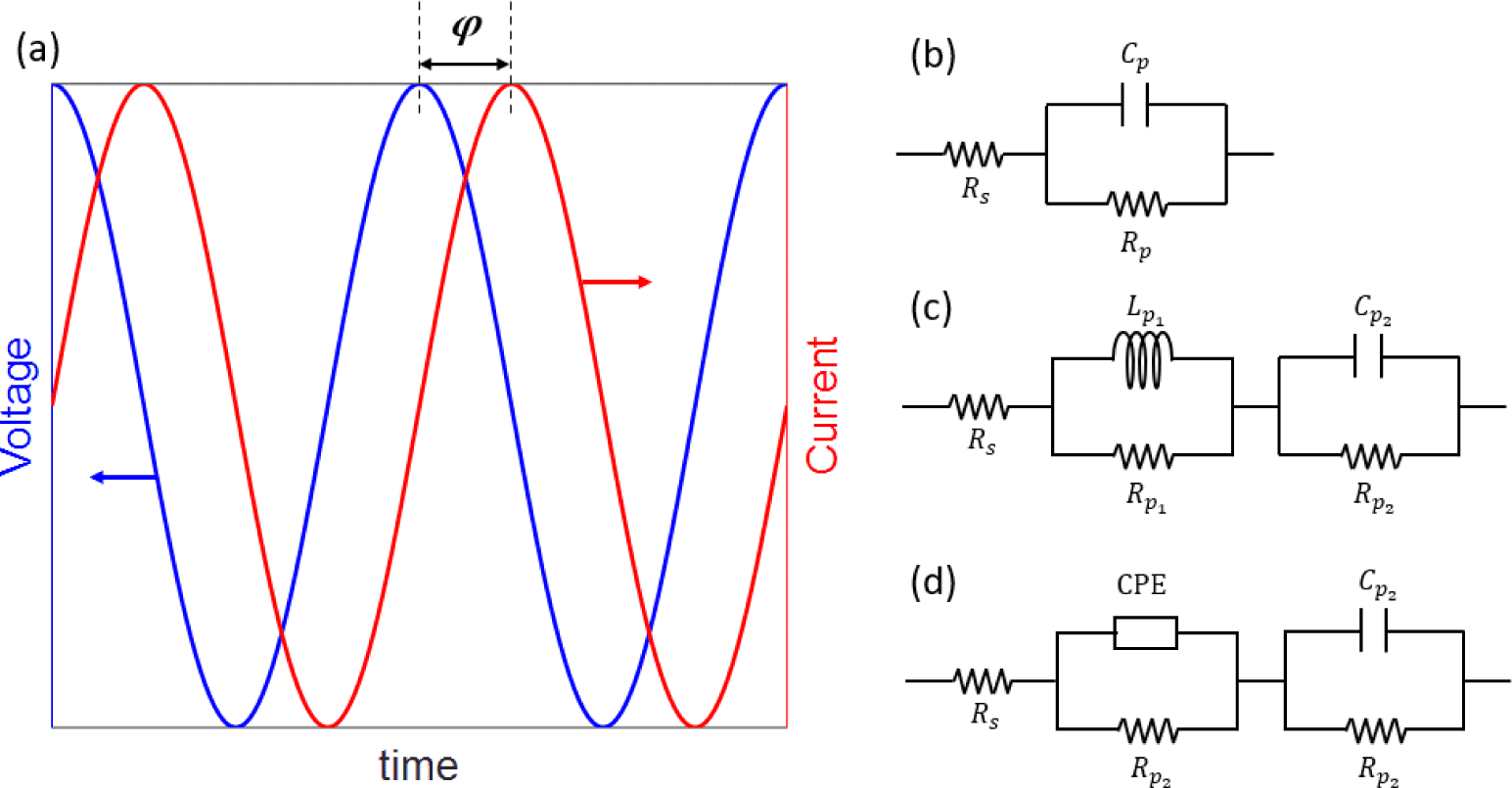
Impedance analyzers typically provide the magnitude Z0 and phase angle φ, from which the real and imaginary components of Z(ω) or Y(ω) can be determined. Because capacitance is not measured directly, it must be extracted from impedance data using an appropriate equivalent circuit model.
The simplest and most widely used model represents the device as a series resistance followed by a parallel resistor–capacitor (R–C) branch [38,39], as shown in Fig. 2(b). For the parallel R–C branch, the admittance is given by Y(ω)=1/Rp+jωCp, and thus, the parallel capacitance is given by:
In practical OLED analysis, however, a single parallel R–C model is insufficient to describe the capacitance response over wide voltage and frequency ranges. Real devices often exhibit multiple relaxation processes and NC, necessitating more elaborate circuit representations. For instance, models that incorporate additional branches associated with specific layers or interfaces–such as parallel R–L elements [29] or constant phase elements (CPEs) that represent a distribution of relaxation times [19,28,9]–have therefore been introduced, as shown in Fig. 2(c) and 2(d).
These inductive-like branches are phenomenological representations of slow feedback processes in charge transport or recombination, which can reduce the effective capacitance, and under certain conditions, lead to negative values. Through such extended circuit models, OLED impedance analysis has progressed well beyond the simple parallel-plate capacitor picture, enabling the extraction of parameters related to injection barriers, interfacial trap distributions, space-charge accumulation, and the conditions under which NC emerges [12,28,32,47].
Transient spectroscopy is a time-domain technique that complements impedance spectroscopy but differs fundamentally in how the capacitance is determined [30,40]. In transient measurements, a small voltage step or pulse is superimposed on a dc bias, and the resulting time-dependent current response is recorded and subsequently transformed into an equivalent frequency-domain representation.
The measured current i(t) consists of an instantaneous component associated with the geometric capacitance and a slower relaxation component governed by charge injection, trapping and detrapping, recombination, and space-charge redistribution. Within this framework, the capacitance can be expressed as:
Here, Cgeo is the geometric capacitance that responds instantaneously to the voltage step, and i(t) denotes the delayed transient current arising from charge relaxation processes.
Eq. (3) explicitly shows that both the magnitude and the sign of C(ω) are governed by the temporal evolution of the transient current through the derivative di/dt. For a conventional R–C response, the transient current decays monotonically following the voltage step, such that di/dt〈0 at all times. Under these conditions, the integral term contributes positively to Cgeo , and the total capacitance remains positive.
In contrast, if the transient current exhibits overshoot or non-monotonic relaxation–where the current initially decays but subsequently increases or even reverses sign–there exist time intervals for which di/dt〉0. These segments contribute negatively to the integral in Eq. (3). At low frequencies, where the capacitance is dominated by long-time components of the transient response, such negative contributions are weighted more strongly. As a result, the integral term can partially or fully compensate Cgeo , yielding C(ω)〈0, i.e., NC.
Transient spectroscopy therefore provides more than an alternative analytic route to extract C(ω). Because C(ω) is constructed directly from di/dt, this technique establishes a direct physical link between NC and delayed charge relaxation, explicitly revealing NC as a consequence of a mismatch between the characteristic timescales of internal charge dynamics and the period of the external electrical perturbation.
To interpret impedance spectroscopy data in OLEDs, several complementary analysis methods are commonly used, each of which is also useful for identifying the conditions under which NC emerges [37].
C–V characteristics describe how the effective capacitance varies with applied bias and are used to identify the dominant charge processes in different voltage regimes. As shown in Fig. 3(a), at low bias (~5 V) the device exhibits a nearly geometric capacitance. With increasing bias, enhanced charge injection and accumulation increase the stored charge, resulting in a rise in capacitance. At higher bias, recombination and space-charge redistribution reduce the net charge storage, leading to a sharp decrease in capacitance. In the example shown, the capacitance even crosses zero and becomes negative above a certain voltage, providing a clear signature of NC.
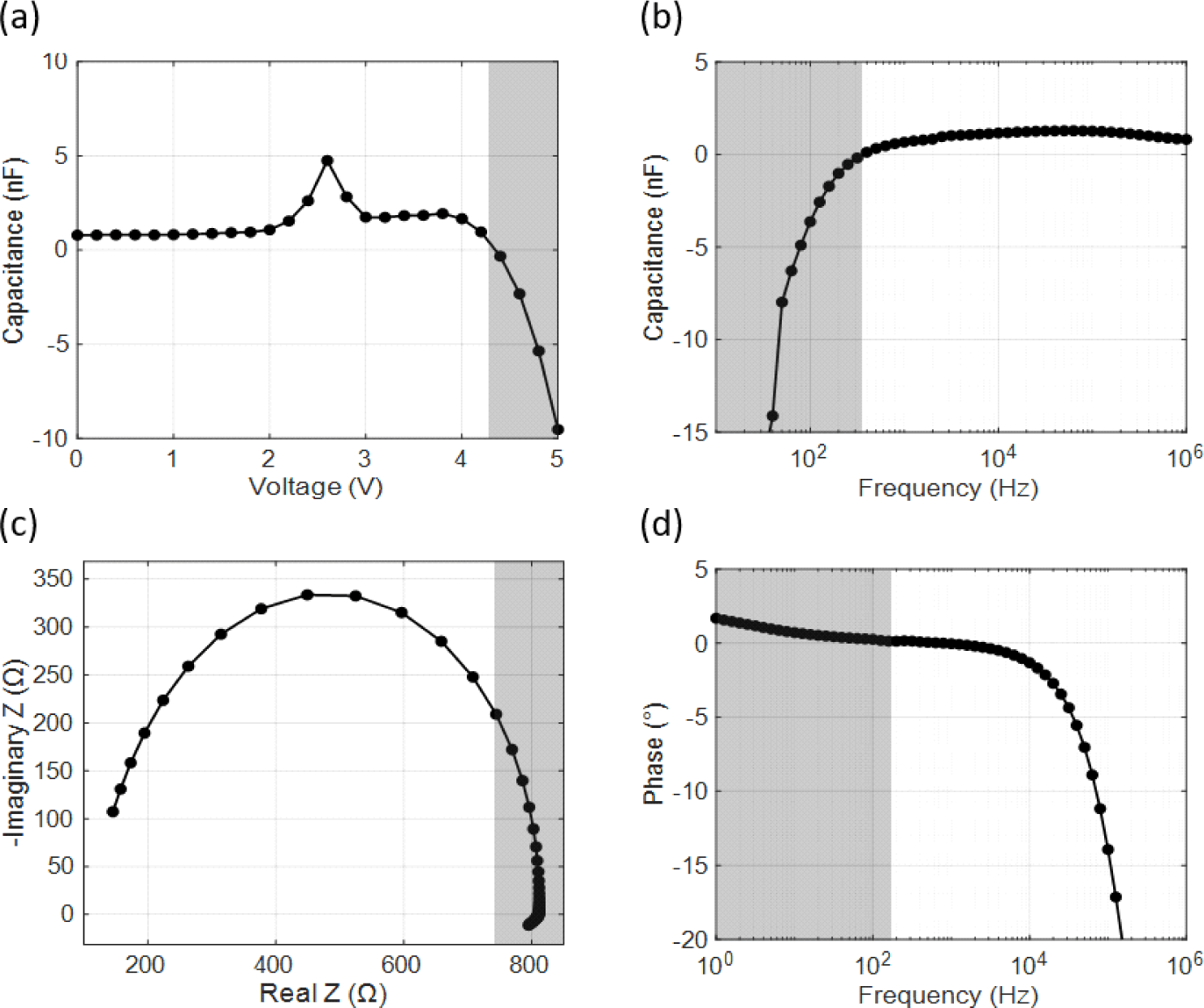
C–f characteristics separate contributions from processes occurring on different timescales. At high frequencies, the response is dominated by geometric capacitance and fast free-charge dynamics; intermediate frequencies reflect interfacial charge accumulation and mobility-related effects; and low frequencies are governed by slow processes such as trap charging, delayed recombination, and self-heating. As shown in Fig. 3(b), the capacitance becomes strongly negative at low frequencies, directly revealing the frequency window in which NC is most pronounced.
Nyquist plots display the real and imaginary components of the impedance in the complex plane. In Fig. 3(c), the impedance traces a semicircle in the capacitive region (positive –Im Z), consistent with a dominant RC response. Near the zero crossing, however, the curve bends slightly into the region where –Im Z becomes negative, indicating an inductive contribution and providing a direct signature of NC.
Bode plots show the magnitude and phase of the impedance as functions of frequency. They directly indicate the frequencies at which the phase deviates from an ideal capacitive behavior and enters an inductive regime. In Fig. 3(d), the phase remains close to 0° at intermediate frequencies but rises above 0° at low frequencies, providing a simple criterion for identifying NC.
Together, the C–V, C–f, Nyquist, and Bode representations provide complementary views of the same impedance data. They enable a comprehensive analysis of charge transport, accumulation, and relaxation across wide bias and frequency ranges, and allow the operating conditions and mechanisms associated with NC to be identified.
3. PROPOSED ORIGINS OF NEGATIVE CAPACITANCE
Numerous studies have attempted to elucidate the physical origin of NC. Broadly, the proposed mechanisms can be classified according to whether the device operates under bipolar and unipolar conditions. In bipolar devices, NC has been attributed to Langevin recombination and trap-assisted Shockley–Read–Hall (SRH) recombination (Section 3.1), injection imbalance between holes and electrons (Section 3.2), charge accumulation at organic–organic interfaces (Section 3.3) and energetic disorder (Section 3.4). Under unipolar conditions, self-heating has been proposed as a dominant origin of NC (Section 3.5).
In this review, we emphasize that NC has most frequently been investigated under bipolar operation, where electron–hole recombination plays a central role. For bipolar devices, NC can be understood from two perspectives: (i) an impedance-based viewpoint, in which NC reflects an inductive-like response arising when internal charge redistribution cannot follow the voltage modulation instantly; and (ii) a charge–voltage viewpoint, in which the extracted capacitance becomes negative when the stored charge decreases despite a constant or increasing bias. To connect these two viewpoints, we consider a reference OLED structure consisting of an anode / hole transport layer (HTL) / emission layer (EML) / electron transport layer (ETL) / cathode, assuming that hole transport is faster than electron transport.
Fig. 4 illustrates how such a mobility imbalance naturally leads to NC. In the initial state (Fig. 4(a)), charges are primarily stored at the electrodes, with negligible charge density in the organic layers. Upon applying a forward bias (Fig. 4(b)), holes with higher mobility rapidly enter the EML, whereas electron injection from the cathode is comparatively delayed. As a result, holes accumulate near the EML/ETL interface, forming a positive space-charge region (Fig. 4(c)) that partially screens the applied electric field and suppresses further hole injection. When electrons eventually reach the interface, they recombine with the accumulated holes, releasing the space-charge (Fig. 4(d)). Because this charge reduction lags behind the applied bias, the device exhibits an inductive-like response manifested as NC.
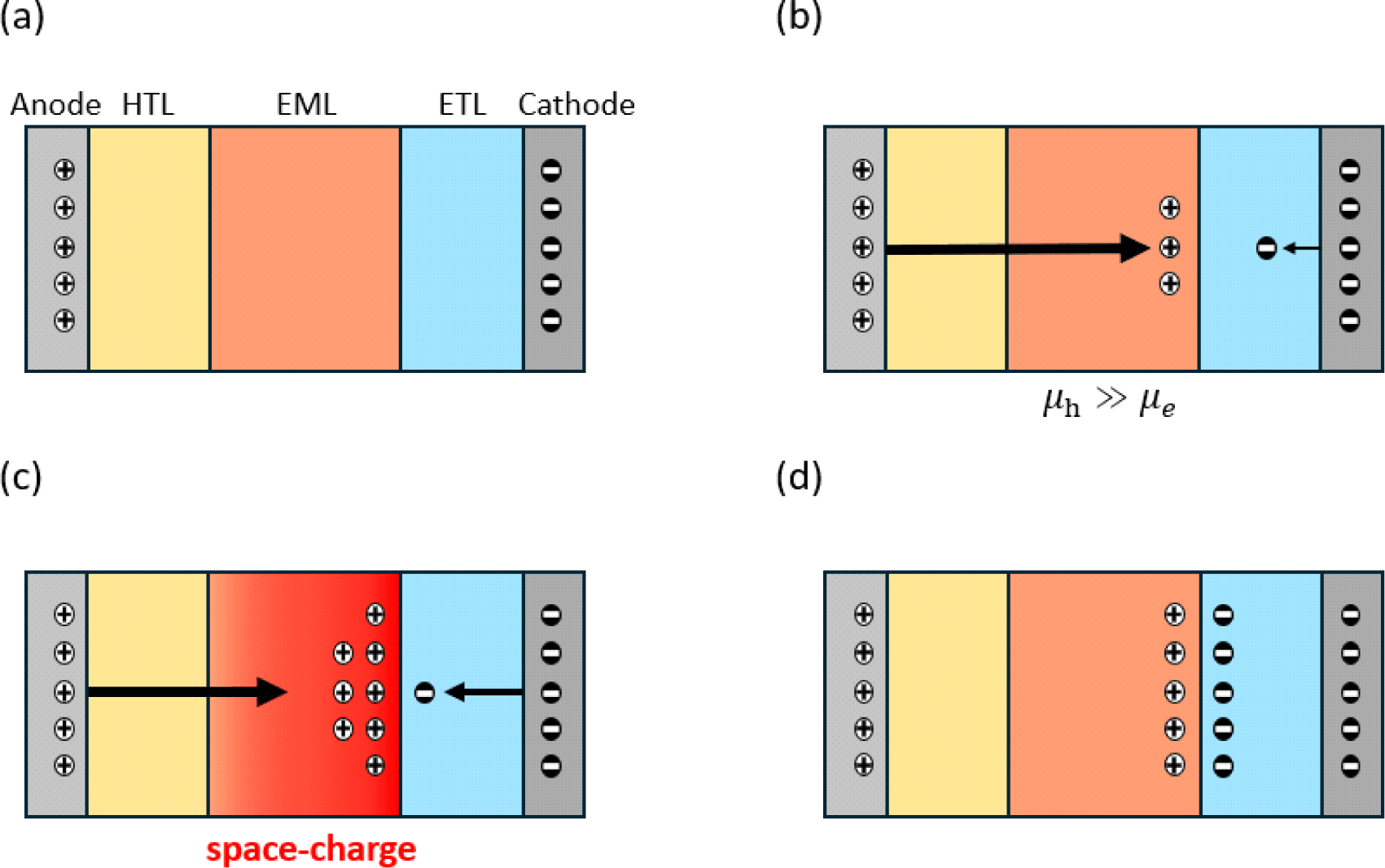
From the charge–voltage perspective, a voltage increase initially raises the stored charge due to hole accumulation. When delayed electron arrival triggers recombination, however, the stored charge decreases even though the applied voltage remains constant (see Fig. 4(c) and 4(d)). Thus, a small increase in voltage (dV/dt〉0) can coincide with a decrease in stored charge (dQ/dt〈0), yielding a negative incremental capacitance, C=dQ/dV.
Table 1 summarizes NC mechanisms by operating condition, frequency/bias regimes, and temperature dependence, providing practical criteria for identifying the dominant mechanism under a given set of conditions.
NC in organic devices arises predominantly under bipolar operation, where electron–hole recombination responds more slowly than the applied voltage modulation. Among recombination pathways, Langevin recombination is generally regarded as dominant in disordered organic semiconductors [40,41]. The Langevin recombination rate is given by:
where q is the elementary charge, ɛ is the permittivity, n and p are the electron and hole densities, and μe and μh are the corresponding mobilities.
Because RL scales with (μe+μh)np, any imbalance or delay in carrier transport directly limits how rapidly recombination can respond to voltage changes. When transport is unbalanced, holes are injected and accumulated earlier, forming a positive space-charge region. The delayed arrival of electrons abruptly increases the local product np, enhancing recombination and rapidly depleting the accumulated charge while the applied voltage remains high or continues to increase. Under such conditions, an increase in voltage can lead to a net reduction in stored charge (dQ/dV〈0), such that the Langevin recombination contributes negatively to the capacitance, giving rise to NC [6,28,29,32].
In the presence of traps, NC can also arise from trap-assisted or SRH recombination, in which the trapped charge in localized states recombines with free charge of the opposite sign [19,42]. If electrons are captured in localized trap states and subsequently recombine with free holes, the recombination rate can be approximated as RSRH ≈ Cp Ntp/2, yielding a characteristic relaxation time τr=2/(Nt Cp), where Nt is the trap density and Cp is the hole capture coefficient.
Assuming a single exponential recombination transient jr (t) = −j0 exp(−t/τr), the resulting capacitance can be expressed as . At low frequencies, the second term dominates and is negative, indicating that SRH recombination provides a negative contribution to C(ω).
Experimentally, increasing electron trap density enhances the low-frequency NC and shifts the capacitance minimum to higher bias, as shown in Fig. 5(a) for devices incorporating phenyl-C61-butyric acid methyl ester (PCBM) as electron traps [19]. Conversely, reducing trap density through concentration optimization suppresses the NC behavior, as demonstrated in Fig. 5(b) for the Poly[2-methoxy-5-(2’-ethylhexyloxy)-1,4-phenylene vinylene]:Poly(N-vinylcarbazole) (MEH-PPV: PVK) blends [38]. These observations support the conclusion that trap-mediated delayed recombination contributes directly to NC.
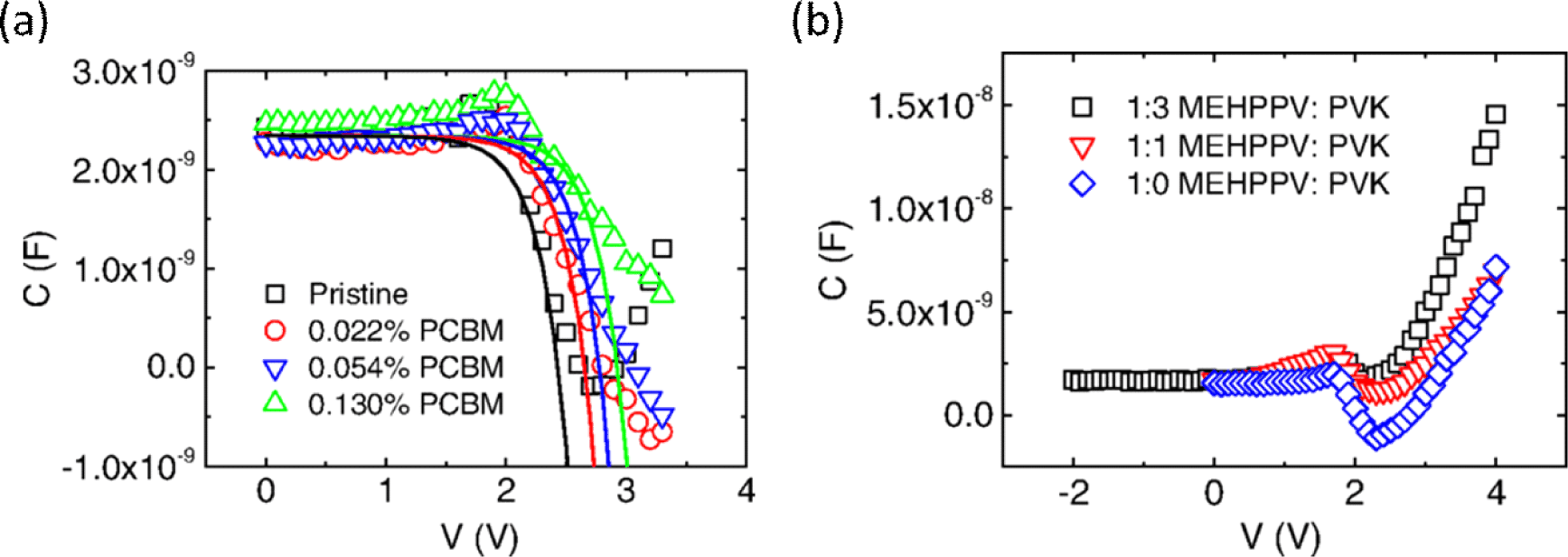
Overall, Langevin and SRH recombination represent closely related pathways to NC. Although their microscopic origins differ, both represent charge removal processes relative to the applied voltage.
Injection imbalance arises due to the energy barriers [43] and interfacial states [12] at metal–organic contacts, playing a crucial role in the emergence of NC. Hole injection at the anode/HTL interface is often nearly Ohmic due to favorable alignment between the anode work function and the highest occupied molecular orbital (HOMO) level of the HTL, whereas electron injection at the cathode/ETL interface is frequently limited by the energy-level mismatch and interfacial states [32,41,4].
Under these conditions, electrons may be temporarily captured in interfacial states before entering the bulk organic layer via tunneling or hopping, introducing a delay relative to hole injection. At low bias, the current is injection-limited; at higher bias, space-charge and bulk transport dominate. Differences in injection barriers, interfacial state density, and relaxation times therefore lead to asymmetric charge injection.
The charge carrier with the lower injection barrier–typically holes–responds rapidly to voltage modulation and accumulates space-charge, whereas electrons arrive more slowly, introducing a lagged current component. This delayed injection imbalance manifests as an inductive-like contribution to the impedance and leads to NC.
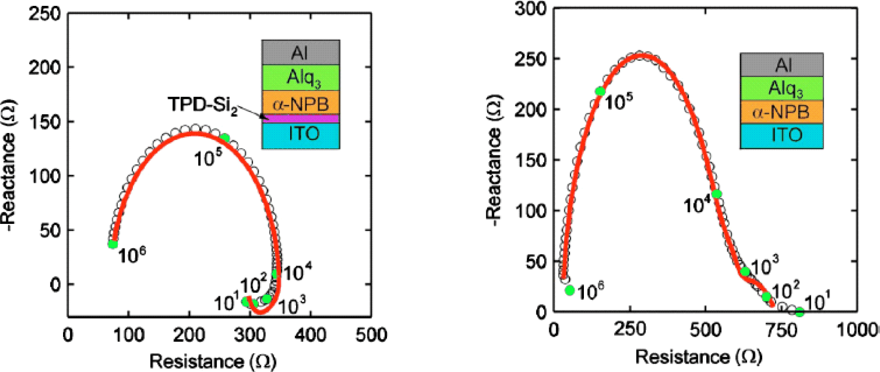
Experimental evidence for this mechanism has been obtained by modifying contact properties [29]. As shown in Fig. 6, introducing a trap-passivation layer 4,4′-bis(N-(1-naphthyl)-N-phenylamino)biphenyl (TPD-Si2) at the anode/HTL interface makes the inductive hook in the Nyquist plot more pronounced and leads to the emergence of negative capacitance (NC). In contrast, in the absence of the TPD-Si2 layer, a capacitive tail appears and NC disappears. This trend indicates that when interfacial traps are reduced and hole injection becomes closer to ohmic behavior, the injection imbalance between holes and electrons is enhanced, thereby making the inductive hook and NC clearly observable. Overall, these results demonstrate that slow, imbalanced charge injection at the metal–organic interface constitutes an independent and significant mechanism for NC.
Charge accumulation at organic–organic interfaces provides another important pathway to NC. Faster carriers–typically holes–arrive first and form a space-charge region that partially screens the electric field, suppressing further charge accumulation until the slower carriers (electrons) arrive. The interface thus serves not merely as a structural boundary between layers but as a dynamic reservoir that temporarily stores and subsequently releases space-charge.
Under a small-signal voltage perturbation, an increase in bias can preferentially trigger the recombination of previously accumulated charges at the organic–organic interface rather than additional charge buildup. In incremental terms, the net stored charge decreases with increasing voltage (dQ/dV〈0), producing NC.
Experimental evidence for the organic–organic interfacial charge contributing to NC has been reported in bipolar OLED structures by systematically comparing C–V characteristics and internal layer configurations, as shown in Fig. 7 [40]. A reference device (D1) containing a single N,N'-di(α-naphth yl)-N,N'-diphenyl-1,1’-biphenyl-4,4’-diamine (NPB) / tris(8-hydroxyquinolinato) aluminum (Alq3) junction exhibits only a shallow NC region. In contrast, devices D2–D4 incorporate additional organic–organic interfaces that serve as extra charge accumulation sites, resulting in multiple inflection points in the C–V curves and a much more pronounced NC regime at higher bias.
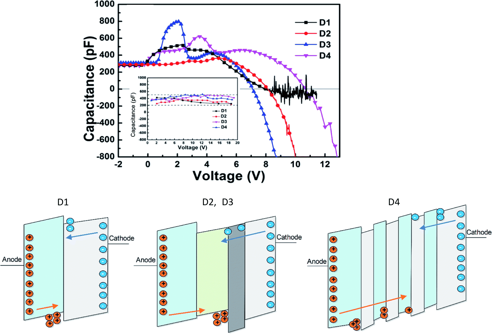
As the number of organic–organic interfaces increases from D1 to D4, a larger amount of charge can accumulate at these interfaces, and the associated relaxation processes become both stronger and slower. Under such conditions, a small increase in bias predominantly drives the release of previously accumulated interfacial charge rather than the additional charge buildup, leading to C=dQ/dV〈0. These observations provide direct experimental proof that delayed formation and release of space-charge at organic–organic interfaces contribute to NC in the impedance response.
Organic semiconductors are typically amorphous and exhibit pronounced energetic disorder in the density of states (DOS), causing carrier mobility and diffusion to depend strongly on electric field and carrier density [45,46]. Under these conditions, space-charge distribution in the bulk cannot adjust instantaneously to voltage modulation but relax through slow diffusion and hopping processes.
Energetic disorder contributes to rapid charge transport through shallow states and slow, trap-limited transport through deep states, giving rise to a broad distribution of relaxation times. Upon a voltage step, charges in shallow states respond quickly along high-mobility pathways, whereas charges in deeper states are emitted more slowly over time. When these fast and delayed responses coexist, there is a frequency range in which the incremental slope of the charge–voltage response, dQ/dV becomes negative, representing NC.
The influence of energetic disorder on NC can be directly examined by varying the disorder parameter, σ/kB T in a bipolar device, as illustrated in Fig. 8 [22]. Here, σ denotes the width of the Gaussian DOS, kB is the Boltzmann constant, and T is the temperature. When the width of the Gaussian DOS is small (σ/kB T≈3), the capacitance at high voltages beyond the C–V peak saturates near the geometric capacitance (Cgeo ) and NC does not appear. In contrast, as the width of the Gaussian DOS increases beyond σ/kB T≈6.5, the capacitance crosses zero after the peak and becomes negative at higher voltages, indicating the emergence of NC.
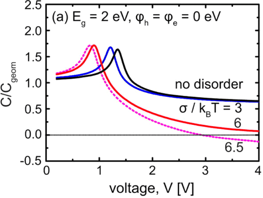
These results show that sufficiently large energetic disorder leads to largely dispersive charge transport, determining both the onset and the magnitude of NC.
Self-heating through Joule heating represents a mechanism for NC that is distinct from purely electronic origins discussed in Sections 3.1–3.4. Joule heating raises the device temperature, enhancing conductivity with a characteristic thermal time constant τch. Because thermal dynamics are slow, conductivity can continue to increase even as the voltage decreases, producing a delayed current response, even in unipolar devices [30,35].
The role of self-heating in NC has been verified through impedance measurements under controlled thermal conditions and by transient experiments. As shown in Fig. 9(a), attaching a high heat-capacity metal block to the backside of the glass substrate to enhance thermal diffusion reduces the magnitude of NC [35]. This reduction indicates that decreasing the delay between the voltage and the temperature/ conductivity response weakens the NC contribution.
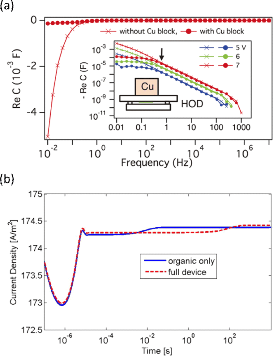
Time-domain transient simulations provide further insight. Fig. 9(b) compares the current response to a small voltage step for two thermal models. In the “organic-only” model, where heat transport is limited to the organic layer, the self-heating-induced current tail develops relatively quickly. In the “full-device” model, which includes the electrodes and glass substrate, the larger thermal mass slows the rise of the excess current [30]. The delayed current, arising from the lag between the applied voltage and Joule heating, manifests directly as NC into the frequency domain. These experimental observations are qualitatively reproduced by drift-diffusion-heat simulations that incorporate the heat equation, supporting the conclusion that NC can arise from self-heating effects.
In this review, we refer electronic NC to NC arising from delayed charge dynamics, including injection imbalance, trapping/detrapping, interfacial space-charge, energetic disorder, and recombination. In such cases, the small-signal current lags the applied voltage because internal charge redistribution cannot follow the modulation instantaneously. In contrast, thermal NC originates from a delayed thermal response. Joule heating raises the device temperature and thereby the conductivity; when the applied voltage is subsequently reduced, the temperature relaxes slowly with a characteristic thermal time constant, producing an inductive-like impedance response in both bipolar and unipolar devices.
Thermal NC is therefore highly sensitive to thermal boundary conditions, which govern heat dissipation, self-heating, and thermal relaxation times. Electronic NC, by contrast, is primarily governed by electronic properties that control charge injection and redistribution, such as transport and injection time scales, trap-assisted relaxation, and bipolar recombination. Because these two forms of NC arise from distinct physical mechanisms, impedance measurements can contain separable thermal and electronic contributions when both thermal relaxation and charge-dynamic delays are active under the same experimental conditions.
4. OUTLOOK
NC in OLEDs provides a sensitive probe of the imbalanced charge dynamics related to injection, transport, trapping, and recombination. In this review, we have summarized how NC emerges in capacitance measurements, how it differs from geometric capacitance, and how it reflects delayed or asymmetric carrier responses at interfaces and within the bulk. Under bipolar operation, the most widely discussed mechanisms–Langevin and SRH recombination, electron–hole injection imbalance, delayed release of interfacial space-charge, and energetic disorder–share a common principle: NC arises when internal charge redistribution lags behind the applied voltage, producing an inductive-like response with dQ/dV〈0.
Despite extensive study of bipolar devices, NC under unipolar operation remains comparatively underexplored. Prior work has mainly attributed unipolar NC to self-heating, where the mismatch between fast electronic response and slow thermal relaxation generates an additional inductive component. However, thermal feedback alone may not capture all potential electronic origins of NC under unipolar operation. Many slow-charge processes identified in bipolar devices–such as trap occupancy modulation, delayed detrapping, injection-limited transport through interfacial states, or dispersive hopping in a broad DOS–are not exclusive to bipolar conditions and in principle, could produce delayed current responses under unipolar operation. Systematic experimental verification and quantitative modeling in these regimes remain limited.
Future studies should focus on carefully designed unipolar devices and biasing schemes to isolate the effects of traps, interfacial states, and energetic disorder from recombination-related contributions. Understanding NC under both bipolar and unipolar operation will open new avenues for diagnosing injection barriers, optimizing interface engineering, and probing slow relaxation processes that are otherwise difficult to detect through steady-state measurements.
In conclusion, NC is not a singular phenomenon arising from a specific mechanism, but a general manifestation of delayed or imbalanced charge response in organic semiconductors. While substantial progress has been made in understanding NC under bipolar operation, extending investigations to unipolar charge dynamics is essential for completing the physical picture. Combining broadband impedance spectroscopy, time-resolved techniques, and advanced multi-physics simulations will be critical to establishing NC as a robust diagnostic probe of charge dynamics and to guiding the rational design of high-performance OLEDs.