PDF Download
 PubReader
 Export Citation
 Email the Author
 Share Facebook
 Share Twitter
 Cited by 0 Article
 Metrics (View:2,723)






1. INTRODUCTION
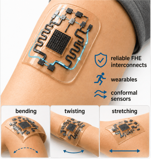
The modern electronics industry is witnessing a profound paradigm shift as form factors transition from traditional rigid, rectangular geometries to complex, soft, and conformable architectures [1]. This evolution is driven by the need for devices that can interface seamlessly with biological surfaces, such as the human body, or wrap around irregular structures for structural health monitoring [1]. At the heart of this transition lies Flexible Hybrid Electronics (FHE), a technology that strategically combines the high- performance computation and communication capabilities of rigid silicon integrated circuits (ICs) with the scalability and mechanical compliance of printed circuitry [1,2]. As outlined in the NextFlex roadmap, this hybridization addresses the inherent trade-off between the high charge-carrier mobilities of monocrystalline silicon (~1,000 cm2/V·s) and the low-cost, large-area manufacturability of solution- processed electronics [1]. The resulting systems, ranging from wearable health monitors and soft robotics to conformal Internet-of-Things (IoT) sensors, require a holistic approach to design that balances electronic performance with extreme mechanical durability [1,2].
Despite the rapid progress in FHE, the interconnection network remains the critical weak link in system-level reliability [2]. Interconnects and vertical interconnection accesses (vias) must not only carry substantial current densities but also survive repeated bending, twisting, and stretching without catastrophic failure [2,3]. This is not merely a material-level selection problem; it is a system-level challenge involving thermo-mechanical coupling and significant mismatches in the coefficient of thermal expansion (CTE) and elastic modulus between rigid dies and flexible substrates [2,4]. To interface the micro-scale contact pads of thinned silicon dies with the macro-scale printed traces, complex redistribution layers (RDL) and fan-out structures are required [1]. These structures often serve as stress concentrators, where the transition from a rigid component (modulus ~100s of GPa) to a soft polymer substrate (modulus ~kPa to 180 GPa) induces high shear and normal stresses, leading to delamination and circuit breakage [1,5,6].
Conventional solutions have relied heavily on silver (Ag) and copper (Cu) nanoparticle (NP) inks, yet these materials face inherent physical limitations. Ag nanoparticle inks, while dominating the market due to their high conductivity and oxidation resistance, are essentially brittle at the system level [5,6]. They typically exhibit channel cracking or grain boundary fracture at strains of less than 5%, which is insufficient for the dynamic 20%–30% strain requirements of skin- wearable applications [4,6]. Furthermore, printed metallic tracks possess a porous microstructure that renders them highly susceptible to electromigration (EM) at high current densities. According to Black’s equation, mass transport is accelerated along grain boundaries and interfaces, causing void formation at the cathode and aggregations (hillocks) at the anode, which eventually precipitates circuit breakdown [4]. Copper NP inks offer a lower-cost alternative but suffer from rapid oxidation under ambient conditions, forming insulating oxide layers (CuOx) that drastically degrade electrical performance and necessitate complex, high-temperature sintering processes that are incompatible with low-thermal-budget plastic substrates like PET [7,8].
Graphene, an atomically thin 2D honeycomb lattice of carbon atoms, has emerged as a formidable candidate to address these deficiencies [9,10]. From a condensed-matter physics perspective, graphene’s charge carriers mimic relativistic particles, described by the Dirac equation as massless Dirac fermions, which enables high carrier mobilities (15,000–100,000 cm2/V·s) and near-ballistic transport [10]. Beyond its phenomenal electronic properties, graphene possesses intrinsic mechanical flexibility and exceptional strength, capable of sustaining elastic strains exceeding 20%—and in some forms, much higher—without loss of functionality [9,11,12]. Its chemical inertness provides stability against oxidation, while its unique structure prevents electromigration at moderate current densities, as the robust sp2 hybridization of the carbon lattice resists the high electron flux that typically displaces atoms in metallic lattices [8,11,12]. Furthermore, graphene’s conductivity can be precisely tuned through chemical doping or hybridization with metallic fillers, which bridge flake-to-flake junctions and reduce contact resistance [8,9].
However, the integration of graphene into FHE faces a fundamental technical hurdle: the conductivity gap. While a pristine single layer of graphene is highly conductive, solution-processed printed graphene networks typically exhibit conductivities that are 10–100 times lower than bulk copper [9,13]. This discrepancy arises from the high resistance at the numerous flake-to-flake junctions within the percolating network, as well as the presence of insulating polymer residues from the ink formulation [7,13]. Navigating this “central tension”—maintaining graphene’s mechanical superiority and chemical stability while pushing its conductivity toward metallic standards—is the core objective of current research and the primary focus of this review.
Fig. 1 provides a schematic overview of this landscape, tracing the transition from Ag/Cu interconnect failure modes to printed graphene percolation networks, the conductivity-gap mitigation strategies discussed in this review, and the target FHE application space.
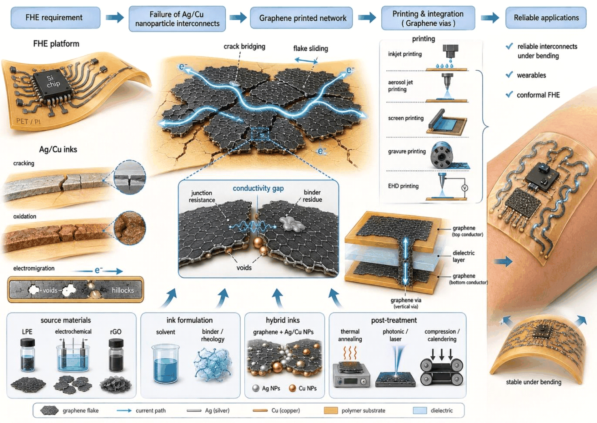
The discussion is organized around the practical demands of FHE interconnects rather than graphene’s intrinsic properties. Starting from the electrical and mechanical requirements that define the design space, it moves through ink formulation — sources, solvents, hybrid systems —into printing method selection, and then into via formation, which receives detailed treatment because it remains the least developed part of the graphene interconnect literature. Conductivity enhancement and mechanical reliability close the discussion. Graphene’s role here is strictly as a passive conductor; its behavior as a transistor channel, transparent electrode or sensing material is left aside, because the design questions are entirely different.
2. GRAPHENE INKS FOR PRINTED INTERCONNECTS
The performance criteria for the interconnects must be revisited when it comes to the FHE. In general, the interconnects in FHE have the role of either power distribution or signal routing.The power distribution interconnect lines should have the sheet resistance less than 1 ohm/sq, otherwise the circuits will face ohmic losses due to Joule heating effect. In the case of signal routing, the sheet resistance values can go up to 10 ohm/sq, since the signal integrity and timing margin are significant here [14]. Conventional printed/sintered copper-based interconnects set the benchmark of ~50 m.ohm/sq at 1 µm thickness, which is very low compared to the graphene interconnects. To close this gap in the performance, graphene interconnects should be optimized based on the sp2 network density and multipass printing [15–17]. It is important to note that, unlike metal interconnects like Cu or Ag (bulk conductivity over 107 S/m), the conductivity in graphene is governed by the long-range ballistic transport within the graphene lattice and the inter-flake junction resistance/flake orientation/percolation pathway, when printed [14,18,19].
Electromigration resistance is equally important to the current carrying capacity in FHE interconnects. At high current densities, the atomic migration takes place in the interconnects, which results in void formation and affects the circuit operations. This void formation is known as electromigration, and the metal nanoparticle-based inks are more susceptible to it. In addition, the thermal mismatch and mechanical strain can also cause degradation of metallic ink-based interconnects. Alternatively, graphene inks-based interconnects are highly resistive to electromigration effect, due to the strong covalent C=C bonds in the graphene backbone [3,20,21].
The mechanical requirements of the interconnects vary based on the specific application. For conformal and flexible electronics, interconnects generally need to withstand moderate bending and strain levels up to approximately 5%. In wearable electronics, the requirement becomes stricter because the interconnects are repeatedly exposed to body motion, bending, twisting, and local stretching; therefore, strain tolerance above 10% is usually required, while high-motion regions such as fingers, elbows, and knees may impose substantially larger local strains [22,23]. Fully stretchable systems are more demanding than flexible FHE, since their reliability is governed mainly by cyclic tensile deformation rather than bending alone. Therefore, endurance over 10,000 bending cycles at a bending radius of 5 mm can be regarded as a useful baseline criterion for flexible and wearable interconnects, but not as a complete reliability criterion for stretchable systems [16,24]. For stretchable interconnects, cyclic stretch–release testing at the target strain level, together with resistance stability under deformation, is also necessary. The mechanical flexibility and high aspect ratio of graphene help to bridge the gaps created during strain-induced deformation. Stress in printed graphene interconnects can also be reduced by placing the conductive layer near the neutral mechanical plane of the multilayer stack.
The mechanical feasibility of the FHE interconnects is also governed by the adhesion of interconnects to flexible substrates, such as polyimide (PI), polyethylene terephthalate (PET), paper and textile. For better adhesion to these substrates the van der Waals forces and mechanical interlocking should work in combination [8,18,21]. More importantly, the surface tension of the conductive ink should match the surface energy of the substrate, which may require a surface treatment step. The native surface roughness of the target substrate also plays a role in adhesion, for example, the PI substrate with higher surface roughness can yield better adhesion than the PET substrate.
The choice of graphene source materials determines the morphology, electrical conductivity and processability of the interconnects. Among several preparation methods, liquid phase exfoliation (LPE) remains the most viable method to produce large quantities of graphene inks with negligible oxidation effects [18,25,26]. In LPE, the delamination of graphite into graphene sheets is achieved by ultrasonication or high-shear mixing. One important point to note is the surface tension of the exfoliation solvent should match the surface energy (~40 mN/m) to achieve maximum exfoliation efficiency. The typical size of graphene flakes ranges from 100–500 nm and thickness can be 2–3 nm (3–8 layers), depending upon the exfoliation duration [17,20,27,28]. In fact, it is the trade-off point, i.e., the higher the exfoliation duration the thinner the graphene sheets (reduced no. of layers), but with the compromise in the lateral size (leads to nanofragments) and defect density. The LPE graphene inks can produce interconnects with conductivity up to 1–5×10⁴ S/m, post annealing. Electrical conductivities over ~105 S/m can be achieved in graphene inks prepared by electrochemical exfoliation (ECE) [13,28,29].
In the ECE protocol, the graphene source solution is prepared by electric current-assisted intercalation of organic/inorganic intercalants into graphite (rod/crystal/ foil), followed by a mild sonication. The ECE process can produce graphene (1–5 layers) with large lateral size up to 10 µm and lowest defect density. Graphene interconnects produced from the ECE graphene inks are suitable for high performance signal routing, however the electrolyte/intercalant removal and scalability challenges remain [17,21].
Reduced graphene oxide (rGO) is the cheapest and highly scalable graphene source, produced by the oxidation of graphite by Hummers’ method. In this process, graphite is oxidized into graphite oxide in the presence of harsh oxidizing agents followed by delamination into graphene oxide (GO) [19,30,31]. The aqueous dispersibility of GO is excellent, suitable for high throughput printing. The bottleneck with GO is the presence of sp3 hybridized carbon and large amount of oxygen functional groups caused by the Hummers’ oxidation process. A post-synthesis reduction step (chemical/thermal/photonic) can greatly reduce the oxygen moieties and restore the sp2 hybridization in the graphene lattice to some extent. The graphene source after this reduction step is known as rGO [11,19]. Though the conductivity of rGO cannot match the LPE or ECE graphene, it is suitable for thick film applications processed by bulk deposition. It’s further important to note that, there is a persistent gap between the intrinsic and practical conductivities of graphene. Fig. 2 summarizes the principal graphene production routes from graphite: the direct liquid-phase exfoliation family (probe sonication, shear mixing, electrochemical, wet-jet milling) and the oxidative GO/rGO pathway, each carrying distinct trade-offs in defect density and dispersibility.
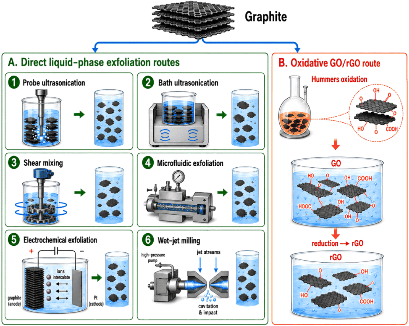
The key differences among these graphene preparation routes are summarized in Table 1. In general, LPE provides low-defect pristine graphene flakes with moderate conductivity and good compatibility with inkjet and aerosol jet printing. ECE can produce larger flakes with higher electrical performance, but electrolyte removal and process control remain important considerations. In contrast, the oxidative GO/rGO route offers the highest scalability and aqueous processability, although the residual oxygen groups and lattice defects limit the final conductivity. Therefore, the selection of graphene source material should be made based on the required balance between conductivity, defect density, ink stability, printability and production scale.
| Preparation method | Flake size | Defect density | Conductivity range | Scalability | Suitable applications | Ref |
|---|---|---|---|---|---|---|
| Liquid-phase exfoliation (LPE) | 100–500 nm | Very low (pristine); ID/IG ratio typically ~0.17–0.28 | ~1×10⁴ to 5×10⁴ S/m | Highly scalable and cost-effective | High-resolution inkjet and aerosol jet printing for TFTs and antennas | [11, 20, 24] |
| Electrochemical exfoliation (ECE) | 1–10 µm | Moderate; residual oxygen groups (C/O ~5–12) and ID/IG ~0.4–1.9 | Up to ~1×10⁵ S/m for single sheets | Scalable with fast production times | Performance electrodes for organic field-effect transistors and supercapacitors | [17, 25] |
| Hummers’ method (oxidative route) | 0.7–100 µm | High; residual oxygen and lattice vacancies persist post-reduction | Typically,<1×10⁴ S/m; optimized films can reach upto ~8.5×10⁴ S/m | Most cost-effective and bulk-scalable | Bulk deposition for chemical sensors, energy storage, and thick-film composites | [19, 26, 27] |
Note: The listed values are representative ranges and can vary with precursor quality, processing conditions, flake size, defect density, residual functional groups, binder content and post-treatment. Conductivity values refer to practical graphene films or printed structures, not intrinsic single-layer graphene.
The single pristine graphene can reach electrical conductivity over ~105 S/m, but when it comes to the printed interconnects the macroscopic conductivity is dominated by the inter-flake junction resistance [11,18]. An electron in graphene has to navigate through the disordered network, where the tunneling resistance at flake-flake overlap acts as a primary bottleneck. This gap can be narrowed down by maximizing the flake alignment and packaging density.
Graphene ink formulation requires a balance between ink rheology and thermodynamic stability.
The ink formulation process takes place in two major steps, first, exfoliation of graphite using a single or combination of solvents and stabilizers, and then ink preparation with a suitable solvent, binders and additives.
The choice of exfoliation solvents includes N-Methyl-2-pyrrolidone (NMP), dimethylformamide (DMF), ethanol, isopropyl alcohol (IPA)/water, etc. Among these, NMP and DMF are widely used solvents because their surface tension values (~40 mN/m) and Hansen solubility parameters closely match those of graphitic materials. The Hansen solubility parameters are commonly expressed as δD, δP, and δH, corresponding to the dispersion-force, polar-interaction, and hydrogen-bonding components, respectively. For example, DMF has representative values of δD~18.0, δP~9.3, and δH~7.7 MPa0.5, which provide good affinity toward the graphitic lattice [26,32]. NMP and DMF are effective, but problematic solvents because of reproductive toxicity and increasingly strict REACH/EU regulatory restrictions. Other solvents such as ethanol or IPA/water require stabilizers, such as ethyl cellulose or PVP to keep the exfoliated graphene stable, i.e., to contain reaggregation [8,25,26]. CyreneTM (dihydrolevoglucosenone), a cellulose derivative, has now been established as a potential ‘green’ solvent for graphite exfoliation. With better Hansen solubility parameters than NMP, Cyrene exhibits superior affinity to graphene. Cyrene can also serve as an additive to aqueous inks, since its higher viscosity (~14.5 mPa.s) can help to modify the ink rheology and printability [25,26].
In the ink preparation step, the exfoliated graphene solution is transferred to a solvent-binder-additive system in order to achieve the printing rheology. The choice of solvent and binder systems is chosen based on the target substrate and thermal budget. If the substrate can withstand annealing temperatures over 350℃, cyclohexanone solvent with terpineol additive and ethyl cellulose binder is gold standard. Some cases used terpineol, ethyl lactate, ethylene glycol, and propylene glycol as standalone or in combination [20,29,33]. Aqueous graphene inks are prepared and used for substrates that require low-temperature processing. For such cases, surfactants like SDS or Triton X-100 are used to maintain graphene stability [18,30].
The fluid mechanics of the inks remain distinct for different printing methods, and it is extremely important to optimize the ink properties accordingly. The widely used inkjet printing requires graphene inks with viscosity 1–20 mPa.s, and inverse Ohnesorge number (Z) between 1 to 14, in order to ensure stable jetting behavior, controlled droplet breakup, and suppression of satellite droplet formation [15,21]. The printability parameter or the inverse Ohnesorge:
Where, η=viscosity, ρ=density, γ=surface tension, and α=nozzle diameter
Aerosol jet printing accepts a wider viscosity window than inkjet, but the usable range depends strongly on atomization mode: ultrasonic atomization is typically limited to low-viscosity inks, whereas pneumatic atomization can process substantially higher-viscosity formulations. In contrast, screen printing employs paste-like inks with highest viscosity (few hundreds to few thousands of mPa.s) and shear-thinning characteristics, owing to the fundamentally different printing process.
The complementary limitations of metal nanoparticle inks and graphene inks have driven the development of hybrid inks, where metallic fillers improve the electrical conductivity of graphene networks while graphene helps retain mechanical flexibility and chemical stability. Among different combinations, graphene/Ag and graphene/Cu hybrid inks are the most representative systems for printed interconnect applications. Graphene/Ag inks mainly target high conductivity and oxidation-resistant interconnects, whereas graphene/Cu inks aim to reduce material cost while using graphene as a protective and conductive framework to suppress Cu oxidation. Therefore, both systems are discussed below in terms of their conductivity enhancement mechanism, mechanical reliability and formulation limitations.
Ag is known for its exceptional electrical conductivity (~6.3×10⁷ S/m) and better oxidation resistance, compared to other printable metals such as Cu [7,34]. When hybridized with graphene flake network, Ag metal nanoparticles establish a highly conductive pathway within the graphene flake network to boost the overall electrical conductivity of the printed lines. Parallelly, the graphene flake network surrounding the Ag nanoparticles thereby bridges the possible mechanical microcracks and connects the voids within. Furthermore, the interconnect lines printed with Ag-only inks suffer from the electromigration effects at high current densities. This effect is greatly suppressed when Ag-nanoparticles are hybridized with graphene, as the latter act as a matrix to hold the Ag nanoparticles and ensure long term conductive stability [16,35].
Cu can reach the bulk electrical conductivity nearly equal (~5.9×10⁷ S/m) to Ag, at substantially lower material cost compared to Ag [7,16,34,36,37]. However, the major bottleneck is the oxidation susceptibility of Cu nanoparticles. Even at ambient conditions, Cu NPs can react with oxygen and form poorly conductive Cu2O/CuO surface layers / a poorly conductive surface layer. In the formulation of Graphene/Cu hybrid inks, graphene (or rGO) flake network can encapsulate the Cu NPs and act as a diffusion barrier for oxygen to reach Cu nanoparticles. This protective framework helps in preserving the Cu metallic core, which in turn improves the overall electrical stability and conductivity [20,38].
The electrical performance and mechanical reliability of the interconnects printed using these graphene/metal hybrid inks is governed by the conductivity-flexibility trade-off. In general, increased metal loading can increase electrical conductivity by improving conductive percolation; however, excessive loading can lead to metal nanoparticle aggregation and rapid sedimentation [16,39]. Such aggregation of metal nanoparticles results in poor printability of the inks and produces brittle interconnects. When maintaining a balance in the graphene-metal nanoparticle ratio, graphene flakes can act as a mechanical scaffold and maintain the durability of the metallic core, while retaining the percolative pathways during deformations.
3. PRINTING TECHNIQUES FOR GRAPHENE INTERCONNECTS
Graphene can be used in flexible hybrid electronics (FHE), to create electrically functional patterns deposited with geometric precision, reliability, and speed. While conventional subtractive microfabrication uses harsh chemicals and high thermal budget processing steps, which are incompatible with polymer substrates like PET and PEN. In contrast, the additive printing techniques offer a low-cost, maskless, and digitally reconfigurable alternative for fabricating flexible electronic architectures [20,40,41]. The printed interconnect applications require a balance between high spatial resolution (for dense signal routing) and sufficient film thickness (for low-resistance power delivery) [42].
Inkjet printing has emerged as a widely adopted method for printing complex device layouts and multilayer electronic architectures with high material utilization efficiency. In particular, the piezoelectric drop-on-demand (DOD) variant has been outstanding for graphene-based electronics due to its ability to produce precise microscale patterns while accommodating broad range of ink formulations [15,43].
The resolution of patterns printed by inkjet printing is determined by the droplet volume (1–10 pL) and the wetting behavior of the substrate. The typical printing resolution of a DOD inkjet printer is reportedly 30–50 µm, and in some cases, it can go upto 20 µm line width upon careful optimization of the ink rheology, substrate surface energy, and printing parameters [27,41,43]. Interestingly, ejection of single spherical droplets can be achieved by tuning the piezoelectric actuation waveform, particularly the pulse rise and fall times, which can eventually minimize the formation of satellite droplets.
In the inkjet printing process, the primary challenge to be addressed is the coffee-ring effect, which results in non-uniform and ring-like printed patterns. It is a hydrodynamic phenomenon that originates from rapid solvent evaporation, where outward capillary flow transports the suspended graphene flakes toward the pinned contact line during droplet drying [27,44,45]. For graphene inks, coffee-ring suppression is usually achieved by controlling the internal flow of the droplet, the evaporation rate, and the ink–substrate wetting behavior. Therefore, the main mitigation strategies can be grouped into three approaches: Marangoni-flow engineering, substrate-temperature control, and substrate-wettability modification.
The first strategy to mitigate the Coffee-ring effect is, creating an inward flow within the printed droplet to counteract the outward capillary flow. This inward flow is known as Marangoni flow, and it can be created by the surface tension gradients that originate when using the binary or ternary solvent systems such as cyclohexanone and terpineol [13,20,46]. The Marangoni flow helps to homogenize the suspended flakes/particles in the printed ink droplet.
During the printing process, increasing the platen temperature (for e.g., 40 to 100℃) can accelerate the solvent evaporation, which in turn can ‘freeze’ the flakes and droplet geometry [45,46].
Another important strategy is the modification of the substrate wettability. The substrates with high wettability behavior will cause the spreading of printed droplets thereby increasing the possibility of coffee-ring effect. In contrast, when substrate wettability is decreased using coatings like HMDS, the droplet spreading is constrained and therefore the target printing geometry is maintained [27,47].
The low solid loading of inkjet inks is a major limitation for conductive interconnects. Graphene concentration is usually kept below 1–2 wt% to avoid nozzle clogging and unstable jetting [43,48,49]. Therefore, multipass printing is required to build thickness and reduce sheet resistance. In general, thickness increases with the number of passes and sheet resistance decreases [17,28].
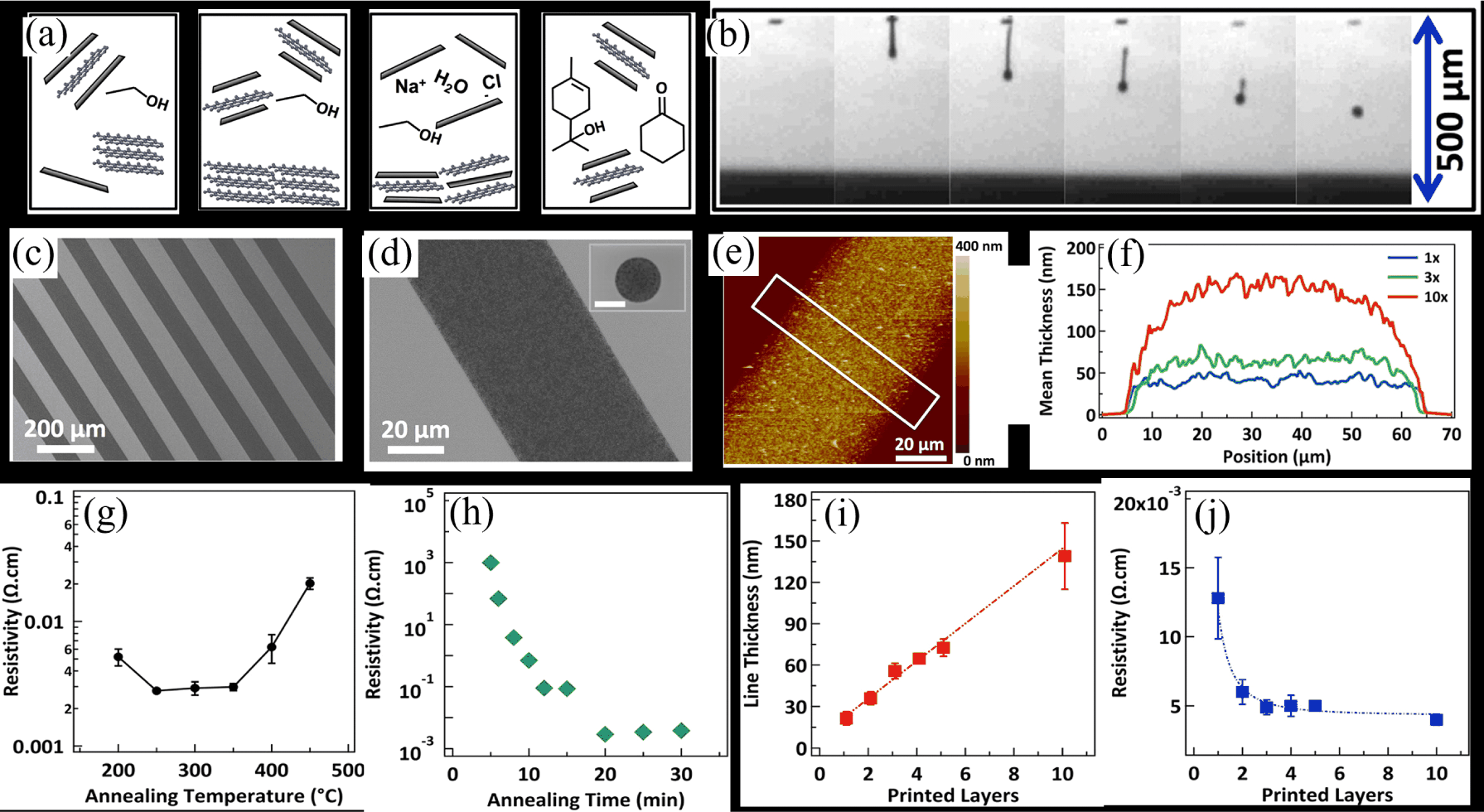
However, too many passes increase processing time, solvent accumulation and the risk of re-dissolving the previous layer. One important point to note is that the graphene flake size must also be controlled to avoid clogging of ink particles at the nozzle. A practical rule is that the graphene flake size should be less than 1/50th of the nozzle diameter. For example, a 20 µm nozzle requires inks with graphene flake size below 400 nm (roughly) [11,15,27]. This requirement improves printability, but it also increases junction resistance because smaller flakes create more boundaries. Fig. 3 shows a representative example of inkjet-printed graphene interconnect formation using an ethyl cellulose-stabilized graphene ink. Fig. 3(a) first describes the complete ink preparation route, where graphite is exfoliated in ethanol/ethyl cellulose by probe ultrasonication, followed by centrifugation to remove large graphite residues, salt-induced flocculation of graphene/ethyl cellulose, and final redispersion in a cyclohexanone/terpineol solvent mixture suitable for inkjet printing. Fig. 3(b) confirms the droplet ejection behavior, showing that stable and nearly spherical droplets are formed after travelling a short distance from the nozzle. The printed-line morphology is then shown in Fig. 3(c)–Fig. 3(e), where SEM and AFM images confirm that uniform graphene features can be obtained without severe coffee-ring formation. The cross-sectional profiles in Fig. 3(f) further show that the printed thickness increases systematically with the number of printing passes, which is important for reducing sheet resistance. The electrical data in Fig. 3(g)–Fig. 3 (j) connect this morphological evolution with the post-processing condition, showing that annealing temperature, annealing time and multipass deposition strongly affect the final resistivity of the printed graphene lines. Therefore, Fig. 3 highlights that ink formulation, droplet stability, multipass printing and thermal annealing must be optimized together to obtain reliable graphene interconnects by inkjet printing [13].
Recent inkjet-printed graphene interconnects have shown conductivities around 2.5×10⁴ S/m using pristine graphene/EC inks [28,49]. Meanwhile water-based electrochemically exfoliated graphene inks have reached around 3.91×10⁴ S/m at approximately 50 µm resolution [17]. These values are useful, but still not metal-like. Inkjet printing is therefore more suitable for signal lines, sensors and moderate-current interconnects than for thick power buses.
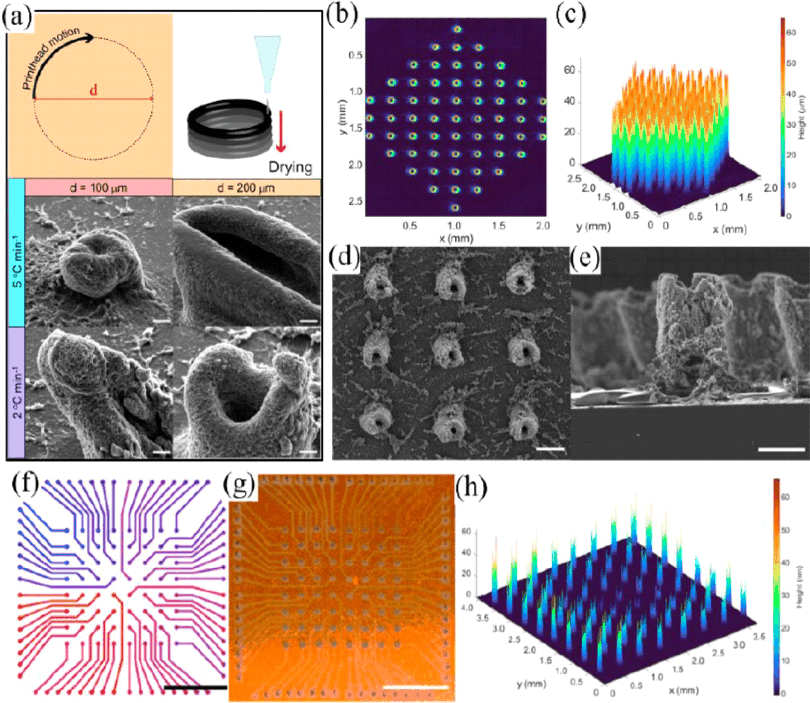
Aerosol jet printing (AJP) is a compelling alternative to inkjet printing, which is more suitable when fine features, high aspect ratio structures or conformal printing over uneven surfaces are required. In AJP, the ink is atomized into small droplets, typically 1–5 µm, and the aerosol stream is focused using a coaxial sheath gas [20,42,50]. This aerodynamic focusing allows a stand-off distance of 1–5 mm, which is a clear advantage over inkjet printing where the nozzle must remain close to the substrate [40,51,52]. Therefore, AJP can print over 3D surfaces, step edges and partially assembled electronic structures. In addition, AJP accommodates a significantly wider viscosity window (1–1000 cP), allowing the use of more concentrated, stable graphene dispersions. This is important because higher solid loading helps to build thickness faster and reduce sheet resistance. AJP is particularly useful for fine-pitch interconnects between rigid chips and flexible substrates, where conventional wire bonding is not suitable. It can also print 2.5D structures such as micropillars with aspect ratios upto 10 [52]. This is where AJP becomes more than a planar printing tool. Fig. 4 shows the capability of aerosol-based printing to move beyond planar graphene lines and form 2.5D carbon interconnect structures. Fig. 4(a) presents the basic additive manufacturing route for carbon pillar formation, where controlled deposition and post- processing are used to build vertical structures with defined diameters. The SEM images in the same panel show that the pillar morphology depends strongly on the printing diameter and heating rate, indicating that solvent removal and structural consolidation are critical for maintaining vertical geometry. Fig. 4(b) and Fig. 4(c) further confirm the formation of an ordered pillar array on a planar electrode using optical profilometry, where the surface map verifies both the height profile and spatial uniformity of the printed structures. Fig. 4(d) and Fig. 4(e) show the top-view and cross-sectional SEM images of graphene pillar structures printed on Kapton, confirming that such 2.5D features can also be fabricated on flexible substrates. Finally, Fig. 4(f)–Fig. 4(h) connect the designed toolpath with the printed electrode array and its corresponding surface profile, showing how the printing path controls the final three-dimensional interconnect geometry. Therefore, Fig. 4 supports the point that aerosol-based printing is useful not only for fine planar interconnects, but also for localized vertical structures and chip-to-flex interconnection schemes in FHE.
The resolution of AJP printed patterns is governed by the focusing ratio (FR), which is given by the ratio between sheath gas and carrier gas. With appropriate focusing line widths of 10–20 µm can be achieved, and in some cases sub-10 µm lines are also reported [18,20,42,50]. However, there are a few drawbacks for AJP; Overspray –during the printing process, small, low inertia droplets escape from the main jet and deposit as sparse satellite spray. This eventually increases the effective line width of the printed pattern beyond the designed limit. One effective way to mitigate this is to saturate the sheath gas with solvent vapor, which in turn reduces the solvent evaporation on the flight and suppresses the overspray. Another bottleneck is the line edge roughness, which can be fixed by optimizing the printing parameters in practice [40,51,53].
Screen printing is the practical workhorse for high-throughput printing of thick power interconnects, ground planes and large-area electrodes. Its main strength is that it can deposit thick films, usually 5–20 µm, in a single pass [54–56]. This makes it more suitable than inkjet printing when the aim is low resistance rather than fine resolution. The method is also compatible with roll-to-roll processing, which is important for industrial production of flexible circuits.
The limitation of screen printing is the resolution of printable pattern. Conventional screen printing usually gives line widths around 50–100 µm, which is mainly due to mesh geometry, paste spreading and stencil limitations [56]. This is not enough for fine-pitch signal routing, but acceptable for power tracks and robust interconnect lines. High-resolution stencils can push the feature size close to 40 µm, but this requires tighter control over paste rheology and printing pressure [57].
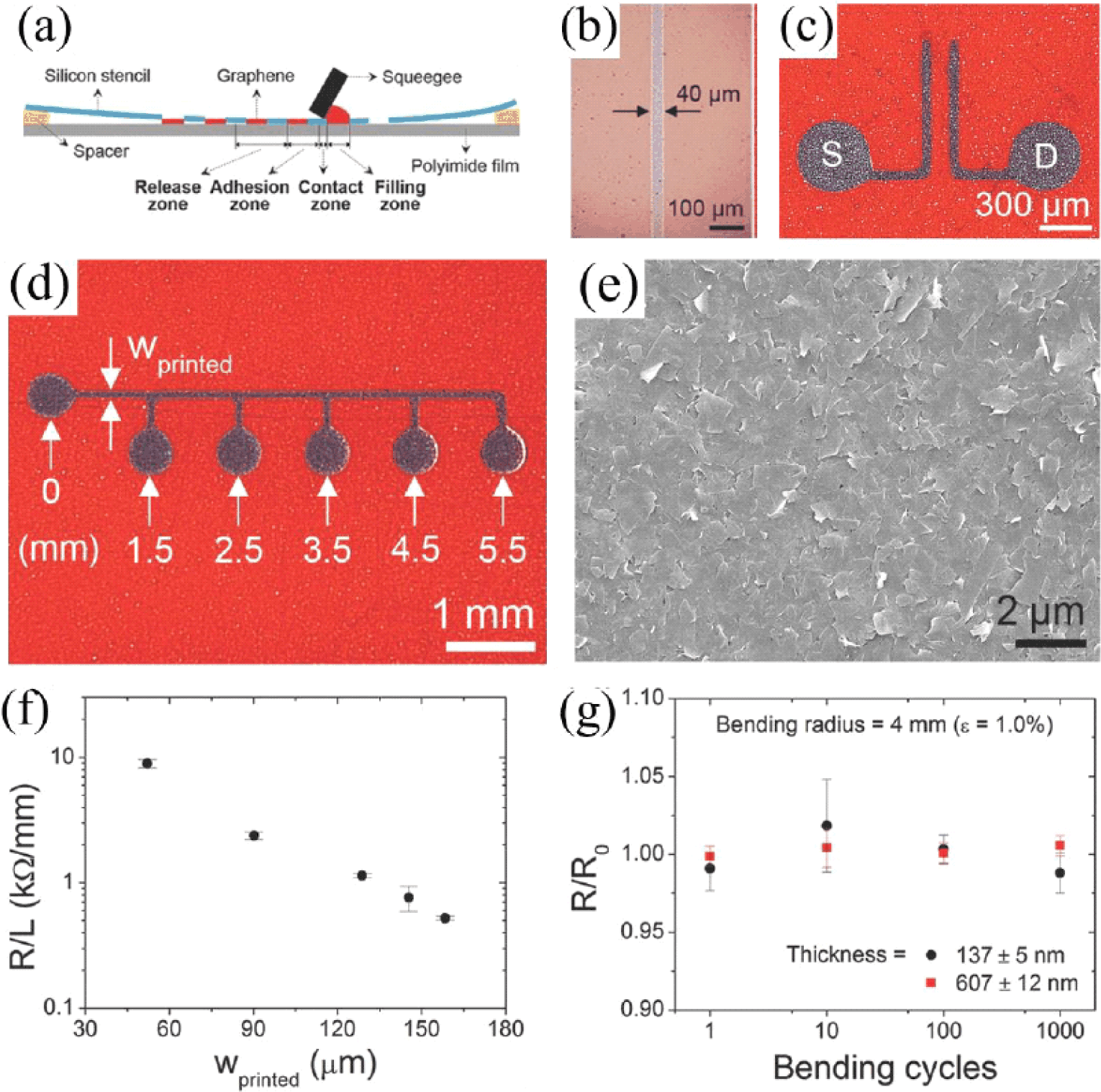
Graphene screen-printing inks are fundamentally different from inkjet inks. They are high-viscosity, shear-thinning pastes, typically in the range of 1–10 Pa․s at moderate shear rate [56,57]. During printing, the paste must flow under the squeegee pressure and pass through the mesh. After deposition, it must rapidly recover viscosity to prevent spreading. This thixotropic behavior preserves the printed line geometry [54,56]. Without it, the paste may be conductive, but the printed pattern will be poor. Fig. 5 shows a representative example of high-resolution screen printing of graphene interconnects on flexible substrates. Fig. 5(a) first illustrates the screen-printing process using a flexible silicon stencil, where the graphene paste is transferred through the patterned opening under squeegee pressure. Fig. 5(b) and Fig. 5(c) show optical microscopy images of the printed graphene lines and source/drain electrodes, confirming that line widths down to 40 µm can be obtained with well-defined printed features. Fig. 5(d) further shows the test pattern used to evaluate the electrical properties of graphene lines with different printed widths and lengths. The SEM image in Fig. 5(e) reveals the morphology of the annealed graphene film, where the flake network forms a continuous conducting pathway after post-treatment. The resistance data in Fig. 5(f) show that the resistance per unit length decreases as the printed line width increases, which is expected from the larger conducting cross-section. Finally, Fig. 5(g) demonstrates the mechanical reliability of the printed graphene lines under repeated bending, where the relative resistance remains stable over 1,000 bending cycles at a 4 mm bending radius. Therefore, Fig. 5 supports the discussion that screen printing is suitable for relatively thick and mechanically reliable graphene interconnects, especially when low resistance and flexible-substrate compatibility are more important than ultrafine resolution [57].
Post-processing is particularly important for screen- printed graphene because the printed film is thick and porous. Compression rolling or calendering after annealing can densify the film, improve flake overlapping and reduce inter-flake contact resistance. Conductivities upto 8.81×10⁴ S/m have been reported for optimized screen-printed graphene films, which is among the higher values for printed carbon conductors [54]. The gain comes from network densification, not from changing the intrinsic graphene itself.
Gravure printing is more relevant when graphene interconnects are considered from a manufacturing viewpoint rather than only from a laboratory prototyping viewpoint. The main advantage of this technique is its direct compatibility with roll-to-roll (R2R) processing, where the patterned ink is transferred continuously from an engraved cylinder to a flexible substrate. The process involves three basic steps: filling of the engraved micro-cells with ink, removal of excess ink from the cylinder surface using a doctor blade, and transfer of the retained ink to the substrate through the nip pressure between the gravure roll and impression roller. Therefore, the final printed feature is not only determined by the ink formulation, but also by the cell geometry, doctoring condition and ink release from the engraved cavity [8,29].
The ink rheology governs the transfer quality in gravure printing. Unlike screen printing, gravure requires relatively low-viscosity inks, typically in the range of 0.05–0.2 Pa·s, so that the ink can fill the engraved cells and detach cleanly during the nip-transfer process [8]. If the viscosity is too low, the ink can spread uncontrollably after transfer and result in edge blurring. If the viscosity is too high, the cell emptying becomes incomplete and the printed line becomes discontinuous. For graphene inks, ethyl cellulose (EC)-stabilized pristine graphene flakes in high-boiling solvents such as terpineol have been widely used because this combination provides sufficient dispersion stability, controlled drying and acceptable film formation. One important point to note is that the surface energy matching between the ink, engraved cell and substrate also controls the transfer efficiency. The interfacial energy is generally tuned close to the graphitic surface energy, around 40 mJ/m2, to reduce the work required for ink detachment from the cell [29,43].
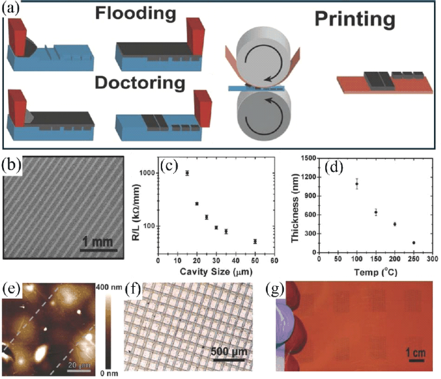
The formation of a continuous graphene line in gravure printing is different from that in inkjet printing. In gravure, the printed line is built by the merging of many small ink volumes released from individual engraved cells. Therefore, the cell-spacing- to-cell-size ratio becomes a critical geometrical parameter. A small spacing-to-size ratio, around 0.1, helps neighboring droplets merge into a continuous wire without leaving gaps between the deposits. However, excessive spreading can also compromise the line resolution. This is the trade-off point in gravure printing—the ink must spread enough to form a continuous conductive pathway, but not so much that the printed line loses edge definition. Fig. 6 shows how gravure printing converts a low-viscosity graphene ink into continuous conductive patterns through cell filling, ink release and post-printing densification. Fig. 6(a) first illustrates the three basic steps of the gravure process: flooding of the engraved cells with graphene ink, removal of excess ink by doctor blading, and transfer of the retained ink to the substrate during printing. Fig. 6(b) shows the printed graphene pattern, confirming that continuous lines can be formed when the ink release and cell geometry are properly controlled. The line-resistance data in Fig. 6(c) further show that the cavity size directly affects the electrical resistance of the printed features, because larger cavitiescan transfer a greater ink volume and form thicker conducting paths. Fig. 6(d) highlights the strong thickness contraction during annealing, which is caused by solvent removal and partial decomposition of the ethyl cellulose stabilizer. This shrinkage is useful to some extent because it densifies the graphene network and improves flake-to-flake contact. The AFM image in Fig. 6(e) shows that the final printed line is very thin compared with the substrate roughness, indicating why surface morphology and ink wetting are critical in gravure-printed graphene lines. Finally, Fig. 6(f) and Fig. 6(g) demonstrate printed crossbar and large-area patterns, showing the relevance of gravure printing for scalable and patterned graphene interconnect fabrication. Therefore, Fig. 6 supports the discussion that gravure printing is attractive for high-throughput graphene patterning, but its electrical performance depends strongly on cell design, ink transfer efficiency and annealing-induced network densification [29].
The as-printed graphene films obtained by gravure are usually very thin, often in the range of 100–200 nm before annealing. During thermal treatment, partial decomposition and removal of the polymer stabilizer cause strong vertical shrinkage, and the final film thickness can reduce to nearly 15% of the original value, typically around 15–30 nm. This thickness reduction is not only a geometrical change. It also densifies the graphene network and improves inter-flake contact, which is important for lowering the sheet resistance. Optimized gravure-printed graphene lines have shown conductivities around 104 S/m and stable electrical continuity over hundreds of bending cycles. The conductivity is still far below metal interconnects, but the method offers a practical route for high-throughput graphene patterning on flexible substrates [29].
Electrohydrodynamic (EHD) printing occupies a different space compared to inkjet, aerosol jet and screen printing. It is mainly useful when the required feature size approaches the fine-pitch region of ultra-thin chip integration and high-density signal routing. In conventional inkjet printing, the droplet size is strongly linked to the nozzle diameter. In EHD printing, the ink ejection is driven by an electric field rather than only by pressure or piezoelectric actuation. When a sufficiently high voltage is applied between the nozzle and substrate, the liquid meniscus deforms into a Taylor cone, and a very small jet or droplet is extracted from the cone apex. This allows the printed feature size to become much smaller than the nozzle diameter. This is the main reason EHD printing can reach sub-10 µm, and in some cases nearly 1 µm, pattern resolution [3,15,41].
The ink requirement for EHD printing is also different from that of conventional direct writing. The ink must be sufficiently conductive or polarizable to respond to the electric field, but it should not become unstable during jet formation. Low-viscosity Newtonian inks, often below 500 mPa·s, are generally preferred because they allow stable cone-jet operation and controlled deposition. For FHE interconnects, this becomes important in two ways.
First, EHD printing can produce very narrow conductive lines for fine-pitch redistribution. Second, it can be used for vertical interconnect access formation, where small ink volumes must be deposited accurately into micro-via openings. This is particularly useful for Ag nanoparticle inks with particle sizes of 3–8 nm, which can fill small step heights more reliably than highly viscous extrusion pastes [3,41].
For graphene-based patterns, the main advantage of EHD-related printing is the possibility of aggressive dimensional scaling. Recent EHD-assisted and maskless transfer-printing approaches have demonstrated graphene line widths around 3.2 µm with spacing close to 1 µm. This is a significant improvement over conventional inkjet-printed graphene, where the line width is usually limited to tens of micrometers. The high resolution is achieved by controlling the wetting and dewetting of the graphene ink on smooth hydrophobic molds, such as Cytop- coated silicon. In this case, the mold does not only define the line width, but also improves the line edge roughness, which can be reduced to below 25 nm. This level of edge control is important when printed graphene is used near chip pads or dense interconnect layouts [41].
The electrical performance of EHD-templated graphene patterns is also promising. Sheet resistance values around 35±6 ohm/sq have been reported for 10 µm graphene lines, while the patterns maintained stable performance under cyclic bending at about 1% tensile strain. It is important to note that this strain value is not a stretchable-electronics benchmark, but it is relevant for fine-pitch interconnects near rigid chip interfaces where the local strain must be minimized. Therefore, EHD printing should not be viewed as a high-throughput replacement for screen or gravure printing. It is better positioned as a high-resolution printing method for local interconnects, chip-to-flex interfaces, micro-vias and fine redistribution layers.
Its practical limitation is throughput and process complexity, but its strength is precision. This makes EHD printing an important tool for scaling graphene-based FHE toward higher circuit density [41]. The major printing techniques for graphene-based interconnect fabrication are compared in Table 2. In general, inkjet printing is suitable for digital prototyping and multilayer layouts, but its low film thickness per pass limits its use for low-resistance power lines. AJP offers better resolution and conformal printing capability, making it useful for fine-pitch die routing and non-planar surfaces. Screen printing is more suitable for thick, low-resistance interconnects and high-throughput fabrication, whereas gravure printing is attractive for large-area roll-to-roll manufacturing. EHD printing provides the highest patterning resolution and is therefore useful for micro-vias and ultra-thin chip integration, although its throughput remains limited. Therefore, the selection of printing techniques should be based on the required balance between resolution, film thickness, conductivity, throughput and substrate geometry.
| Technique | Viscosity Window | Resolution | Thickness per Pass | Reported conductivity | Throughput | Best-fit application | Ref |
|---|---|---|---|---|---|---|---|
| Inkjet printing | 1–30 mPa·s | 20–50 µm | <200 nm | 3.91×10⁴ S/m | Moderate (digital) | Digital prototyping and complex multi-layered layouts | [13, 17] |
| Aerosol jet (AJP) | 1–1,000 mPa·s | 5–20 µm | 100–700 nm | ~5×10⁴ S/m | Moderate (digital) | Conformal printing on 3D/curved surfaces and fine-pitch die routing | [20, 44, 51] |
| Screen printing | 1–10 Pa·s | 40–100 µm | 5–25 µm | 8.81×10⁴ S/m | High (roll-to-roll) | Power buses, ground planes, and high-volume manufacturing | [55, 57] |
| Gravure printing | 50–200 mPa·s | ~30 µm | 15–30 nm | ~1×10⁴ S/m | Very High (up to 15 m/s) | Large-area, industrial-scale high-speed production | [32, 44] |
| EHD printing | ≤500 mPa·s | 1–10 µm | Nanoscale | 35±6 Ω/sq (sheet Res.) | Low (high-res focus) | Micro-VIAs, ultra-thin chip integration, and nanoelectronics | [3, 42] |
4. VIA FORMATION AND 3D INTERCONNECTS
The progress from single-layer flexible circuits to complex multilayer FHE requires reliable vertical interconnect access structures. Without vias, flexible circuits remain mostly limited to planar routing, which increases footprint and prevents compact integration of ultra-thin chips, sensors and antennas. In rigid microelectronics, through-silicon vias (TSVs) and electroplated copper structures are matured technologies. In flexible substrates, the same approach cannot be directly transferred because the substrates are soft, thermally limited and mechanically unstable under bending [2,3,58].
The substrate is the first limitation. PI is widely used in flexible printed circuits because it has high thermal stability, with glass transition temperature above 400°C, and good chemical resistance [1,59]. But PI is relatively expensive and often needs laser drilling or aggressive patterning steps. PET and PEN are cheaper and transparent, but their thermal budgets are much lower, generally around 80–120°C for PET/PEN-type processing windows. This makes high-temperature sintering difficult. Paper and textile substrates introduce another issue: the porous network absorbs the ink and disturbs via filling unless a planarization layer is used. Therefore, the via process must be designed around the substrate, not only around the conductive ink.
Poor step coverage is the most common failure mode in printed vias [1,4,59]. In an electroplated Cu via, the metal can be grown thick and continuous along the sidewalls. In printed vias, the ink has to wet the sidewall, fill the via mouth and remain continuous after solvent evaporation. During drying, the film shrinks and stress concentrates near the via collar. This can produce cracks, delamination or discontinuity at the sharp edge of the hole. High aspect ratio vias are even more difficult because viscous inks may coat the upper wall without reaching the bottom. This gives an apparently filled via, but electrically the connection is unstable [60].
Printing-based via formation usually starts with hole formation followed by conductive ink infiltration. CO2 lasers at 10.6 µm are commonly used for PI because the polymer absorbs strongly at this wavelength. The drawback is that thermal ablation can leave carbonized residues and a heat-affected zone. Ultrashort pulsed (Picosecond and femtosecond) lasers reduce this problem by cold ablation, producing cleaner microvias with diameters upto 10 µm and sharper edges [58,61]. The laser step determines the via wall quality, which in turn determines the ink filling quality.
Once the through-hole is formed, ink infiltration is governed by wetting, viscosity and drying dynamics. The ink must flow into the via during deposition, but it should not slump or drain out before solidification. The non-Newtonian and Shear-thinning inks are useful because they have low viscosity under printing stress and regain viscosity after deposition [2,62]. Layer-by- layer inkjet filling can be used for prototyping, but the coffee-ring effect becomes severe inside the confined via geometry. Flakes can move toward the via edge and leave the center under filled. This increases contact resistance and causes early failure under current stressing.
AJP is a stronger method for high-aspect-ratio via filling because the focused aerosol beam can deliver material into recessed or non-planar regions without direct nozzle contact. Phase-inversion graphene inks are particularly interesting in this context. By adding a low-volatility nonsolvent such as glycerol, the ink can change from a low-viscosity aerosol-compatible state to a gel-like deposited state after impact. This gelation process prevents the collapse during drying and allows 2.5D pillar structures with aspect ratios upto 10 [52]. The important point is that the via is not filled only by volume deposition; it is stabilized by an ink rheology transition.
Graphene-metal hybrid vias are used because pure graphene vias usually lack the raw conductivity required for dense power routing. In hybrid vias, Ag or Cu provides the main conductive path, while graphene acts as a crack-bridging and mechanically compliant interface [63]. During bending or thermal cycling, metallic nanoparticle films can develop microcracks. Graphene flakes can bridge these cracks and maintain percolation across damaged regions. Hybrid graphene/Ag structures can therefore give much lower resistivity than pure graphene while maintaining better fatigue resistance than metal-only vias.
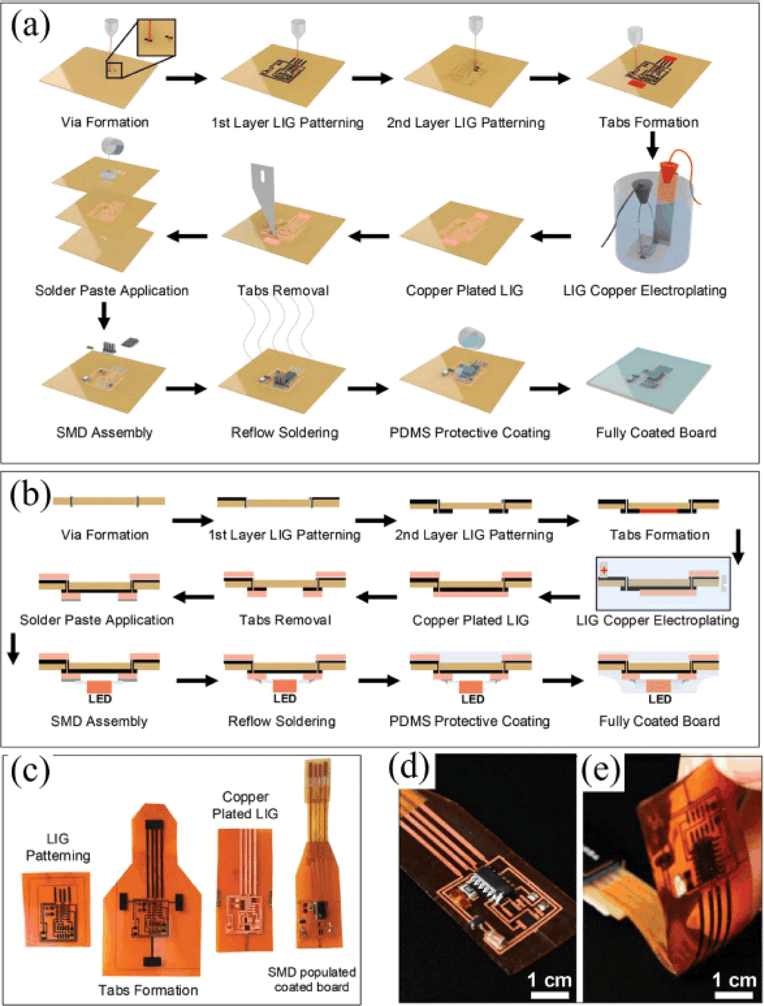
Laser-induced graphene (LIG) offers a different route for vertical interconnects [64,65]. Instead of printing an external ink on a PI substrate, a CO2 laser irradiation can convert the sp3 carbon in PI into porous sp2-rich graphene under ambient conditions. In a double-sided flexible circuit, the laser can ablate a hole and carbonize the rim of the via at the same time, forming a conductive ring between the top and bottom layers. Bare LIG is relatively resistive, around 50 ohm/sq, but it works well as a porous seed layer for copper plating. When Cu is deposited into the LIG framework, the resulting Cu-LIG composite can approach 1.67×10⁶ S/m conductivity [64,66]. This is not purely a graphene via anymore. It is a graphene-assisted metal via. Fig. 7 shows a representative route for forming double-sided flexible printed circuits using laser-induced graphene followed by metallization. Fig. 7(a) first presents the overall E-LIG fabrication sequence, where graphene patterns are generated on both sides of the polyimide substrate, followed by via and tab formation, copper plating, tab removal, solder paste deposition and SMD assembly. This process flow is important because it shows that laser-written graphene can act not only as a printed conductor, but also as a seed layer for subsequent metal reinforcement. Fig. 7(b) gives the corresponding cross-sectional view of the structure at different fabrication stages, clarifying how the top and bottom conductive layers are connected through the via region. The photographic images in Fig. 7(c) show the practical progression of the flexible PCB from the original polyimide substrate to the intermediate and final fabrication stages, which confirms the process compatibility with large-area flexible substrates. Finally, Fig. 7(d) and Fig. 7(e) show the assembled double- sided flexible PCB and the operating LED on the bottom layer, demonstrating that the formed interconnects and vias can support functional device integration. Therefore, Fig. 7 supports the discussion that graphene-based via structures can be used as part of a hybrid interconnection strategy, especially when combined with metal plating to reduce resistance and improve circuit-level reliability [64,67].
Other 3D graphene structures, including graphene foams and laser-sintered porous carbon architectures, are also being explored for vertical interconnects. Their high porosity and mechanical compliance can help absorb bending-induced strain in system-in-foil architectures [65,68]. However, these structures are still far from standardized interconnect technologies. The immediate practical route is more likely to be hybrid via structures, where graphene contributes mechanical stability, oxidation resistance or crack bridging, while metal provides the main current path.
Though the early printed vias reportedly suffered from high contact resistances, recent progress has shown noticeable improvements. For example, the optimized EHD and extrusion based silver vias have achieved resistance values as low as <2 ohms, for the step heights of 4 µm [3]. In the case of AJP graphene interconnects, the power dissipation is reportedly limited by the thermal resistance of polymer substrate, and therefore the thermal-aware design is highly important in 3D integration [69].
5. CONDUCTIVITY ENHANCEMENT, MECHANICAL RELIABILITY AND INTEGRATION
The electrical performance of printed graphene interconnects is limited in the as-deposited state. Freshly printed films contain solvent residues, polymer stabilizers, voids and weak flake-to-flake contacts. Therefore, post-processing is essential to convert a printed carbon coating into an interconnect. The main aim is to remove insulating residues, increase packing density and reduce the inter-flake tunneling barrier [28,70].
Thermal annealing is the conventional method for conductivity improvement. The useful temperature range is defined by the substrate thermal budget.
PET is generally limited to less than 150°C, PEN to less than 200°C, while PI can tolerate 350–400°C. Paper substrates are usually kept close to 100°C to avoid charring [2,28,54,70]. This means the same graphene ink can give different conductivities on different substrates, simply because the binder cannot be removed equally.
The improvement during annealing comes mainly from binder decomposition, solvent removal and flake coalescence. EC, PVP and similar stabilizers surround the graphene flakes and create a dielectric barrier between them. When the film is heated, these organic components decompose or volatilize, and the flakes come into closer contact. In some cases, aromatic carbon residues can assist π-π interaction between flakes and act as a weak conductive bridge. Thermal annealing can improve conductivity by 10–100 times, often pushing the film above 104 S/m [13,24,49]. While the incomplete annealing leaves residues, too aggressive annealing damages the substrate.
Photonic annealing is useful when the substrate cannot withstand long thermal exposure. For example, intense light sources such as xenon flash lamps to heat the printed graphene filmwithin milliseconds. Graphene absorbs light strongly, so the printed trace can reach temperatures above 250°C while the bulk polymer substrate remains comparatively cool [12, 70, 71]. This selective photothermal heating is especially useful for PET and other low-temperature foils. The risk is non-uniform heating if the film thickness or optical absorption is not uniform. Fig. 8 shows the role of photonic annealing in improving the conductivity of printed graphene interconnects on both flexible and rigid substrates. Fig. 8(a) first illustrates the intense pulsed light (IPL) annealing process, where short high-energy light pulses are used to locally heat the printed graphene pattern without exposing the whole substrate to a high thermal budget. This is particularly important for polymer substrates, where conventional thermal annealing can cause deformation or thermal damage. Fig. 8(b) shows optical images of inkjet-printed graphene patterns on different substrates such as Beyolex, PEN, Kapton and fabric, confirming that the same post-processing route can be applied across mechanically different flexible platforms. The sheet-resistance comparison in Fig. 8(c) shows that the substrate thermal conductivity strongly affects the photonic annealing response, since low-thermal- conductivity polymer substrates retain heat differently from rigid substrates. Fig. 8(e) further shows the effect of pulse energy on sheet resistance, indicating that the annealing energy must be optimized to remove insulating residues and improve graphene network connectivity without damaging the film. Fig. 8(f) compares the normalized sheet resistance after photonic and thermal annealing on different substrates, showing the advantage of photonic processing for temperature-sensitive substrates. Finally, Fig. 8(g) shows the thickness-dependent sheet resistance of graphene/nitrocellulose films, confirming that both film thickness and annealing method control the final electrical performance. Therefore, Fig. 8 supports the point that conductivity enhancement in printed graphene interconnects is not governed only by the graphene source, but also by the post-processing route, substrate thermal properties and printed-film thickness [70,72].
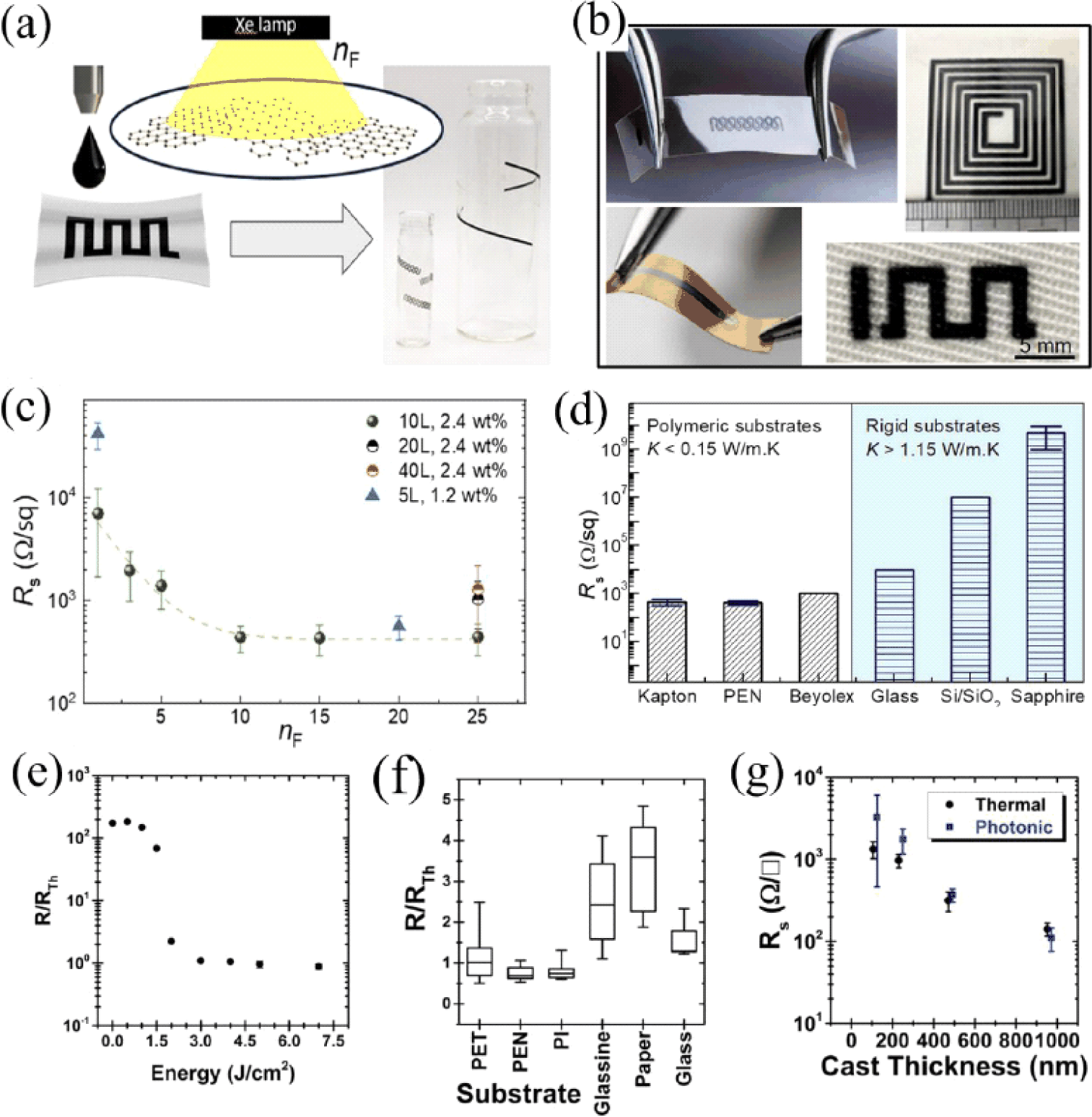
Laser processing provides even more localized treatment. By controlling the laser fluence, the printed trace can be annealed, sintered or partially graphitized without heating the whole substrate [6,66]. In LIG processing, the same principle is extended to directly convert PI into porous graphene. Photonic and laser treatments are attractive for roll-to-roll manufacturing because they are fast and compatible with ambient processing. However, they require careful energy control. Too little energy leaves the binder behind, while too much energy burns the film or deforms the substrate.
Mechanical compression/calendaring are useful in improving the electrical conductivity of printed FHE interconnects, by addressing the inherent porosity of the printed graphene flakes. The printed patterns/film are densified by applying pressure through a roller, which eventually increases the flake to flake overlapping and decreases the inter-flake distance of non-contacting flakes to within the tunneling regime (<3 nm) [54,73]. This physical lamination yields a conductivity improvement of 2–5x, and in binder-free systems, the enhancement can be upto 50x. The advantage of calendering is that it does not depend strongly on substrate temperature. The limitation is that excessive pressure can damage soft substrates or crack brittle underlying layers.
Chemical doping is another route to reduce resistance. Acids such as HNO3 or dopants such as AuCl3 can increase hole concentration in graphene and lower sheet resistance [6,54]. The improvement can be large, but stability is the main problem. Many dopants are sensitive to ambient moisture, oxygen or heat, and the conductivity can degrade over weeks or months. Therefore, chemical doping is useful for demonstrating high conductivity, but it is not automatically a reliable manufacturing solution. Combined treatments such as calendering followed by thermal or photonic annealing are often more realistic because they improve both network density and residue removal.
The mechanical robustness of the printed interconnects is characterized by the relative change in resistance (ΔR/R0) as the function of bending radius (rc) of the substrate. Unlike bulk metals interconnects and transparent oxides, graphene-based printed interconnects maintain electrical robustness at extreme radii (<2 mm) [13,49]. The conventional metal-based interconnects exhibit failure or unpredictable resistance changes after 750–1000 bending cycles, due to irreversible crack formation. However, graphene-based interconnects can withstand 1500–10,000 cycles, with resistance variation less than 5% [24,54,66]. This performance flexibility is attributed to the percolated graphene network. In other words, when a substrate with graphene interconnect undergoes deformation or bending, the graphene flakes slide over each other to maintain the electrical contact within. Furthermore, establishment of new tunneling junctions under deformation helps to retain the original electrical conductivity.
The stretchable interconnects need to overcome the mechanical mismatch between the printed interconnects and the elastic substrates. The conventional metal interconnects fail when stretched, due to the channel cracks perpendicular to the strain [6,74]. In the case of graphene, the crack paths can be deflected by the percolated graphene network, and it can undergo stable, serrated failure when reinforced with specific binders. The printed interconnects can withstand strain over 100% when the structural strategies such as serpentine geometries, kirigami patterns and/or pre-strained (PDMS, TPU) are used [6,75]. These strategies help to decouple the global elongation of the substrate from the local material stress.
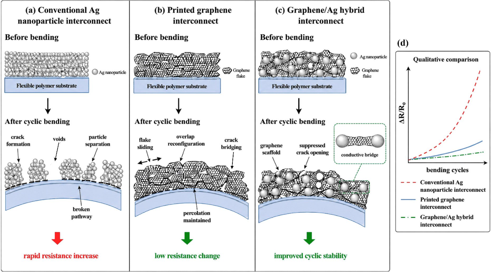
Environmental stability of the printed interconnects is essential to maintain reliability, since humidity and temperature cycling can change the resistance by swelling the binder, oxidizing metal fillers or weakening adhesion at the substrate interface. The choice of binder can determine the stability of the interconnects, for e.g., nitrocellulose binder has shown good resistance stability under 85°C/85% RH damp heat testing, whereas ethyl cellulose based interconnects tend to degrade up to 50% [2]. Encapsulation of printed interconnects with stable polymer films, such as PI or silicone can protect them from moisture and oxygen attack, which in turn can expand their lifespan without appreciable degradation [76]. The mechanical advantage of graphene-based interconnects compared with conventional metal nanoparticle interconnects is summarized in Fig. 9. In conventional Ag nanoparticle interconnects, repeated deformation can induce crack formation, particle separation and void growth, leading to rapid resistance increase. In contrast, printed graphene networks can accommodate deformation through flake sliding, overlap reconfiguration and crack bridging, thereby maintaining the conductive percolation pathway. In graphene/Ag hybrid interconnects, the graphene scaffold further bridges separated Ag nanoparticles and suppresses crack opening, providing a balance between enhanced conductivity and improved cyclic stability.
The use of printed graphene in FHE depends not only on the printed line itself, but also on how it connects with rigid silicon chips, metal pads, dielectrics and encapsulation layers. This interface between soft printed conductors and rigid components is often the weak point in the system. A graphene interconnect may be mechanically robust, but the device can still fail at the chip pad, solder joint or via contact.
Interfacing rigid IC pads with printed graphene requires low-temperature bonding. Conventional Sn-Pb solders exceedthe thermal budget of many polymer foils, while Sn-Bi solder and anisotropic conductive films (ACF) can operate around 100–150°C [1,2]. Graphene can also act as a solder-compatible barrier when printed over Ag traces. During soldering, Ag can dissolve or react with flux, which weakens the contact [77]. A graphene overlayer can reduce this degradation and maintain a stable interface. This is a useful role because graphene is not only acting as the conductor, but also as a protective interfacial layer.
Printed graphene can also function as a redistribution layer (RDL) or fan-out interconnect. Ultra-thin silicon chips can have pad pitches below 50 µm, while large-area printed circuits usually have much coarser resolution [2]. The RDL bridges this geometry mismatch by redistributing fine chip contacts to wider printed traces. This is an important application area for AJP and inkjet printing because both can create localized patterns without full-area lithography.
Multilayer FHE circuits require printed dielectrics and reliable vias. PVP, SU-8 and PI are commonly used as insulating layers, while Ag, graphene or hybrid inks form the interconnect levels [1,3,66]. AJP is particularly useful for sequential deposition of ground planes, dielectric layers and sensing/interconnect layers. However, registration accuracy remains a serious issue. If the alignment error is on the order of tens of micrometers, the via may miss the pad or the printed conductor may short with the adjacent layer. Therefore, multilayer printing is not only a material problem. It is a registration and process-control problem.
Graphene-based FHE demonstrations are most convincing when the material advantage is connected to the device requirement. Wearable electrophysiological sensors use graphene because of its flexibility, large surface area and reasonable skin compatibility [24,77]. Biochemical sensing platforms use graphene because the surface is sensitive to ionic and molecular interactions. Flexible RFID antennas and paper-based RF tags use graphene because bendability and lightweight form factor are more important than absolute metal-like conductivity [54,73]. The field should avoid presenting graphene as a universal replacement for Ag or Cu. Its stronger position is in mechanically demanding, chemically sensitive and low-temperature printable systems where metals alone face reliability limitations.
6. SUMMARY AND OUTLOOK
The central challenge of printed graphene interconnects in FHE is not one of intrinsic material capability—it is the persistent gap between what a single graphene flake can do and what a disordered printed network actually delivers. This review has examined that gap from every practical angle. On the ink side, EEG-derived flakes with large lateral dimensions and low defect density offer the highest printed conductivity, reaching upto ~105 S/m, but scalability and electrolyte removal remain unresolved. LPE graphene is the more widely deployed source, which reliably produces interconnects in the 1–5×10⁴S/m range after annealing, which is sufficient for signal routing but not for power delivery. rGO closes the cost barrier, at the expense of a permanently disrupted sp2network that no amount of reduction fully restores. Across all three, the inter-flake junction resistance is the bottleneck, and closing it requires not just better flakes but better network architecture. Hybrid graphene/Ag inks represent the most practical near-term solution: Ag nanoparticles fill the inter-flake gaps and lower percolation resistance, while the graphene scaffold bridges microcracks and suppresses electromigration. The conductivity-flexibility trade-off in these systems is real, but it is manageable when the graphene-to-metal ratio is matched to the application —leaning graphene-rich for mechanically demanding wearable routes, and metal-rich for static redistribution layers.
On the printing side, no single method dominates. Inkjet printing is well-suited to signal routing at 20–50 µm resolution, but coffee-ring suppression through Marangoni flow engineering and substrate temperature control remains essential for achieving uniform film coverage. Aerosol jet printing is the method of choice for fine-pitch chip interconnection and via filling, enabled by its wide viscosity window and standoff- distance advantage, though overspray management and registration accuracy over large areas are still limiting factors. Screen printing remains the most productive route for power bus fabrication, delivering thick graphene films with conductivities approaching ~104–105 S/m range after calendaring, in which the gains originate from network densification, not from the graphene itself changing. Via formation, the most underexplored area in the graphene interconnect literature, has been treated with particular attention here. Hybrid graphene-assisted metallization, where graphene or LIG provides a mechanically compliant seed or crack-bridging interface and copper provides the primary conductive path—represents the most promising direction for achieving practically viable vertical interconnects in multilayer FHE stacks. Pure graphene vias remain too resistive for current-dense applications. Mechanically, printed graphene interconnects maintain ΔR/R0 below 5% over 1,500–10,000 bending cycles depending on ink formulation and structural design, substantially outperforming sintered metal NP films, whose resistance rises sharply and often irreversibly after fewer than 1,000 cycles. The mechanism is not crack resistance—it is percolation reconfiguration: flake sliding, new junction formation and distributed current rerouting. This is the genuine materials advantage of graphene over metallic nanoparticle systems in mechanically dynamic FHE.
Graphene-based printed interconnects are not yet replacing silver nanoparticle inks at scale. The conductivity gap remains real, the processing infrastructure is less mature and the reliability database is thinner. Their stronger position, for now, is in mechanically demanding, thermally constrained and chemically sensitive applications where sintered metal films have already been shown to fail.
Several open problems define the direction of this field going forward. The most fundamental is the junction resistance problem. Inter-flake junctions remain the rate-limiting step in printed graphene conductivity, and while thermal annealing, photonic sintering and calendering each address it partially, none provides a manufacturing-compatible, substrate- agnostic solution. The emerging idea of chemical junction welding using π-conjugated bridging molecules or conformal metal coating at flake edges to create covalent or near-ohmic flake contacts has shown promise at the laboratory scale, but translation to roll-to-roll compatible processes is not established. MXene/graphene co-deposition is another direction worth watching: MXene’s metallic conductivity and 2D morphology make it a natural junction-filling candidate within a graphene percolation network, and early results suggest the combination can outperform either component alone. More importantly, the second open problem is one that the field rarely acknowledges: there is no agreed benchmark for printed via resistance. Without a standardized test structure, such as specifying aspect ratio, substrate, anneal condition and measurement protocol, comparisons across literature are nearly impossible, and progress on via performance cannot be tracked reliably. This is a field-level gap that slows development more than any specific materials limitation.
Self-healing and damage-tolerant design represent a near-term opportunity that remains largely unexplored for printed interconnects. Graphene percolation networks reconfigure passively under deformation, but active recovery through encapsulants that refluidize at body temperature or through microcrack-triggered conductive healing agents—has not been demonstrated in a printed FHE context. The materials building blocks for this already exist in soft robotics and self-healing polymer research; the translation to printed interconnect stacks is a realistic short-term goal. Finally, the jump from laboratory-scale printing to roll-to-roll manufacturing remains the real commercialization barrier, and it is predominantly a process engineering problem rather than a materials one. Registration accuracy across large substrate areas, ink stability over multi-hour print runs, drying uniformity in high-throughput web processes and quality control for sub-50 µm features at roll speeds—these are the problems that will determine whether printed graphene interconnects move from demonstrations to deployed FHE products. They deserve considerably more research attention than the field currently directs toward them.