Journal of Flexible and Printed Electronics
Korea Flexible & Printed Electronics Society
REVIEW

발광소자 응용을 위한 양자점 인쇄기술 연구동향

송현화1, 양지웅1,2,*
Hyeon Hwa Song1, Jiwoong Yang1,2,*
1대구경북과학기술원 에너지공학과
2대구경북과학기술원 에너지공학연구소
1Department of Energy Science and Engineering, Daegu Gyeongbuk Institute of Science and Technology (DGIST), Daegu, Korea
2Energy Science and Engineering Research Center, Daegu Gyeongbuk Institute of Science and Technology (DGIST), Daegu, Korea
*Correspondence: jiwoongyang@dgist.ac.kr

Author Contributions

HHS drafted the manuscript. JY supervised this work and finalized the manuscript. All authors read and approved the final manuscript.

ⓒ Copyright 2022 Korea Flexible & Printed Electronics Society. This is an Open-Access article distributed under the terms of the Creative Commons Attribution Non-Commercial License (http://creativecommons.org/licenses/by-nc/4.0/) which permits unrestricted non-commercial use, distribution, and reproduction in any medium, provided the original work is properly cited.

Received: Jul 12, 2022; Revised: Aug 18, 2022; Accepted: Aug 23, 2022

Published Online: Aug 31, 2022

Graphical Abstract

jfpe-1-1-45-g9

ABSTRACT

Colloidal quantum dots (QDs) are promising materials for the next-generation displays, because of their excellent optical properties such as color tuneability, bright emissions, and extremely high color purity. For the practical applications of QD-displays, it is important to develop high-resolution QD printing methods that produce QD pixel arrays. Here, this review article highlights QD printing techniques for applications to light-emitting diodes. We provide an overview of the recent advances and challenges in three representative QD printing techniques: (i) photolithography, (ii) inkjet printing, and (iii) transfer printing. We also discuss how these methods have been applied to fabricate QD light-emitting diodes.

Keywords: Inkjet printing; Photolithography; Printing; Quantum dot; Transfer printing

1. 서론

최근 다양한 광전자 소재를 적용한 차세대 디스플레이 연구가 활발히 이루어지고 있다[1-3]. 수 nm 가량의 크기를 지니는 반도체 나노결정인 양자점(quantum dot, QD)은 밴드갭 제어 가능성, 높은 색순도, 고휘도의 우수한 광학적 특성[4-8]을 나타내기에 차세대 디스플레이 응용에 적합한 물질로 주목받고 있다[9-14]. 또한, 양자점 발광소자는 봉지층을 포함한 소자의 두께를 수 마이크로 이하의 초박형으로 제작 가능하기 때문에 차세대 유연디스플레이로의 응용까지 기대를 받고 있다[15-22]. 따라서, 양자점 디스플레이와 관련된 많은 연구가 활발히 이루어지고 있으며, 산업계에서도 양자점을 사용한 제품의 상용화가 진행되고 있다[23]. 특히, 최근 전계발광 양자점 발광소자(quantum dot light-emitting diode, QLED)에 대해 이론적 한계에 육박하는 외부양자효율을 달성하기도 하였다[24-27].

양자점은 주로 콜로이드 용액상에서 합성되어 용액에 분산되나[4,28], 전자소자에서는 박막 등의 고체형태로 적용하기 때문에 양자점을 박막화하는 공정 기술은 양자점 발광소자 개발을 위해 필수적이다[29-31]. 기존 연구에서는 주로 간단한 과정을 통해 고품질 박막 제작이 가능한 스핀코팅(spin coating)[32,33]을 이용하여 단색 발광소자에 대한 연구가 주로 진행되었으나[9-14], 양자점 디스플레이 기술이 실용적으로 활용되기 위해서는 단색광이 아닌 적·녹·청(red, green, and blue, RGB) 삼원색과 같은 다색의 패턴화된 픽셀을 이용한 소자가 제작되어야 한다. 특히, 최근 웨어러블, 가상 및 증강현실 디스플레이 기술 발달에 따라 요구되는 디스플레이 해상도가 증가하고 있다[34-36]. 따라서, 고해상도의 픽셀을 서로 다른 색상간 교차오염없이 구현할 수 있는 양자점 인쇄기술의 개발이 필요하다.

이에 본 종설논문에서는 포토리소그래피, 잉크젯인쇄, 전사인쇄의 대표적인 3가지 양자점 인쇄 기술에 대한 연구동향에 대해 논의하고자 한다. 각 기술들의 장단점을 살펴보고, 양자점 발광소자로의 응용 대표 사례에 대해 소개하고자 한다.
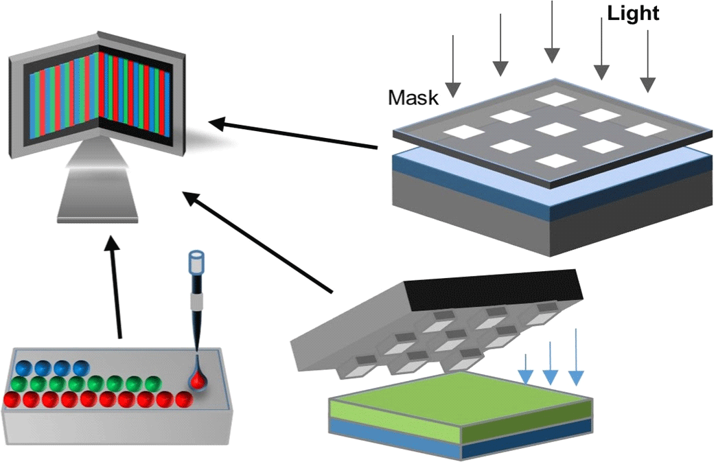
2. PHOTOLITHOGRAPHY

포토리소그래피란 빛과 광마스크를 이용하여 고해상도의 미세화된 패턴을 제작하는 반도체 공정이다. 전통적인 포토리소그래피 공정에서는 빛이 광마스크의 패턴을 따라 감광제(photoresist)의 화학적 반응을 유발한다[37,38]. 이후 현상액(developer)을 통해서 빛에 노출된 영역을 선택적으로 남기거나 제거하여, 최종적으로 기판 표면에 광마스크의 패턴을 남긴다. 이 기술은 이미 산업적인 수준에서 잘 발달되어 있기에 양자점에 적용하기 위한 노력이 꾸준히 이루어져 왔다[39-40].

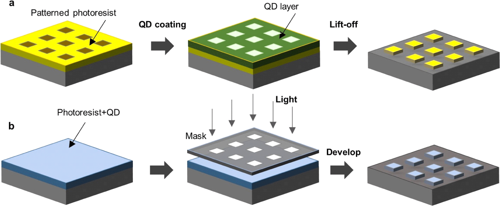
양자점 포토리소그래피는 다양한 형태로 공정이 이루어지고 있다. 대표적으로 패턴 형태의 감광제층 위에 양자점을 코팅하여 lift-off 공정을 통해 원하는 패턴의 양자점을 얻을 수 있다(Fig. 1(a)). 역으로 양자점 층 위에 감광액 층을 도입한 후, 선택적으로 양자점 층과 감광액 층을 제거하여 패턴을 형성할 수 있다. 이외에도 양자점을 감광액과 같은 용액에 잘 분산되도록 표면개질을 하여 양자점과 감광제를 혼합하여 도포하는 방식도 있다(Fig. 1(b)). 양자점/감광제 혼합필름에 광마스크를 통해 빛을 조사하여 현상과정을 통해 원하는 양자점 패터닝을 완성하게 된다.

jfpe-1-1-45-g1
Fig. 1. Schematic illustration showing photolithography of QDs, (a) using a lift-off process and (b) using the mixture of photoresist and QDs.
Download Original Figure

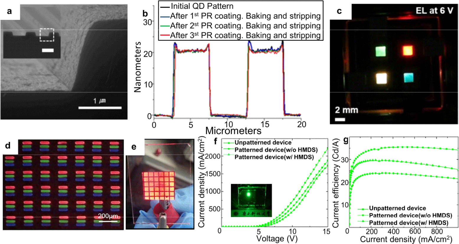
양자점에 포토리소그래피를 적용하기 위해 기존 공정의 개선에 대한 연구들이 많이 이루어지고 있다. 대표적으로 기존 방식을 적용할 시 존재하는 면적과 패턴 해상도 간의 trade-off 관계의 문제점을 layer-by-layer 공정[41]과 포토리소그래피 공정의 결합을 통해 해결한 사례가 있다(Fig. 2(a))[42]. 반복적인 공정을 통해 양자점 층의 두께를 미세하게 제어하면서도 관련된 열화현상은 보이지 않아, 전계 발광소자에 적용 가능하였다(Fig. 2(b)Fig. 2(c)). 또한, 최근 연구에서도 포토리소그래피와 lift-off 공정을 통해서 우수한 소자특성을 성취하였다[43]. 네거티브 광감제인 AZ5214E 를 사용하고, lift-off 공정에서 QD의 손실을 방지하기 위해 ZnMgO층을 hexamethyldisilazane으로 코팅하여 양자점 층과의 부착힘을 증가시켰다. 이를 통해 픽셀화된 양자점 발광소자를 구현하였으며(Fig. 2(d)Fig. 2(e)), 녹색 발광소자기준 29.7 cd/A의 높은 전류 효율을 나타냈다(Fig. 2(f)Fig. 2(g))[44].

jfpe-1-1-45-g2
Fig. 2. QLEDs made by photolithography of QDs, (a) Photograph of the patterned substrate after the layer-by-layer deposition, (b) atomic force microscopy line profile demonstrating minimal damage to the QD layer by the iterative photolithography process, (c) photograph of multi-color QLEDs. Panels (a−c) were reprinted with permission from ref [42]. Copyright 2016 American Chemical Society, (d) fluorescence image of 400 μm× 400 μm RGB pixels consisting of 100 μm×400 μm rectangular sub-pixels, (e) photograph of patterned QLEDs. (f,g) Electroluminescence properties of QLEDs showing the effect of HMDS treatment. Panels (d−g) were reprinted with permission from ref [44]. Copyright 2018 Society for Information Display.
Download Original Figure

포토리소그래피 공정은 저비용으로 원하는 패턴의 양자점을 광마스크를 통해 쉽게 얻을 수 있고, 병렬적 공정특성으로 대량생산에 적합하지만, 에너지가 큰 빛을 사용하기 때문에 양자점의 광퇴화가 발생할 수 있을 뿐만 아니라, 광감제의 사용으로 잔여하는 유기물이 소자의 성능을 저하시킬 수 있다. 따라서, 전통적인 감광제가 아닌 양자점 표면리간드의 반응을 통한 포토리소그래피 기술 개발이 이루어지고 있다. 대표적으로 광산화제 양이온과 음이온 무기리간드의 조합을 이용한 양자점 포토리소그래피 연구가 보고되었다(Fig. 3(a))[45,46]. 빛을 흡수하게 되면 광산화제가 분해되어 수소 이온을 방출하고, 이는 음이온기나 나노입자 표면과 반응하여 양자점층을 경화시킨다. 이 방식은 기존의 감광제를 필요로 하지 않으며, 금속이나 반도체 등 다양한 무기나노결정에 적용될 수 있다(Fig. 3(b)). 패터닝된 픽셀에서 기존의 양자점 용액과 유사한 광발광 스펙트럼을 확인할 수 있으며(Fig. 3(c)), 마스크에 의해서 1 μm 수준의 해상도도 구현이 가능하다.

jfpe-1-1-45-g3
Fig. 3. QD photolithography using surface ligands, (a) mechanisms of QD photolithography using photosensitive cation-anion ligands, (b) photograph showing negative patterns of CdSe/ZnS QDs, (c) photoluminescence spectra of patterned RGB film and QD solutions. Panels (a−c) were reprinted with permission from ref 45. Copyright 2022 American Association for the Advancement of Science, (d) schematic illustration showing the mechanism of QD photolithography using ligand crosslinkers, (e) photoluminescence quantum yield of red-emitting CdSe QD films as a function of added crosslinker contents, (f) electroluminescence properties of QLEDs made by photolithography. Panels (d−f) were reprinted with permission from ref [47]. Copyright 2020 Springer Nature.
Download Original Figure

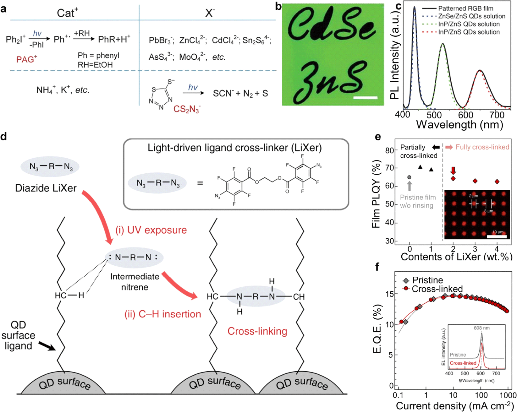
기존 양자점에서 사용되는 유기리간드를 그대로 사용하면서 유기리간드와의 가교결합 반응을 통해 양자점을 패터닝하는 포토리소그래피 연구 역시 보고되었다(Fig. 3(d))[47]. Ethane-1,2-diyl bis(4-azido-2,3,5,6 tetrafluorobenzoate와 같은 빛에 의해 반응하는 가교제가 양자점의 리간드를 서로 맞물리게 되면서 연결시켜 단단한 네트워크를 형성하게 된다. 본 공정에서는 양자점에 혼합되는 가교제의 양을 5 wt% 미만으로도 최소화하고, 0.4 mW/cm2 정도의 약한 빛(파장: 254 nm)을 이용하여서도 양자점 패턴이 잘 형성된다(Fig. 3(e)). 따라서, 본 기술을 통해 양자점의 광학적·전기적 특성에 대한 영향을 최소화하여, 14% 이상의 우수한 외부양자효율을 나타내는 양자점 발광소자를 제작할 수 있었다(Fig. 3(f)).

3. INKJET PRINTING

잉크젯인쇄 기술은 잉크화된 액상 재료를 분사하여 박막을 생성하는 증착 기술로 컴퓨터 프린팅 기술에서 널리 사용되어지고 있다[48]. 콜로이드 양자점은 용매에 분산되어 용액의 형태로 활용이 가능하기에 양자점 용액을 잉크로 사용하여 잉크젯인쇄 기술에 적용하기 위한 많은 연구가 이뤄졌다[49-51]. 잉크젯인쇄 방식은 프린트 헤드 부분에 있는 노즐을 통해서 잉크 방울이 분사되고, 헤드와 기판의 상대적인 위치의 정확한 제어에 의해서 기판의 특정 위치로 잉크 방울이 떨어져 코팅되어지는 원리로 진행된다(Fig. 4(a))[52,53]. 잉크젯 프린팅 방식은 프린트 헤드 부분의 움직임을 통해서 원하는 모양의 패턴을 제작할 수 있으며, 비접촉 방식으로 반복적인 공정이 가능하고, 대면적에 유리하다는 장점이 있다[54,55]. 또한, 최종적으로 제작하고자 하는 모양대로 잉크를 분사하기에 낭비되는 재료를 최소화 할 수 있고, 마스크 또한 필요하지 않아 비용면에서 경제성을 갖춘 기술이다[56]. 따라서 최근에는 잉크젯 인쇄 방식을 활용해 다양한 전자소자를 구현하는 연구가 활발히 진행되고 있다[57].

jfpe-1-1-45-g4
Fig. 4. Inkjet printing of QDs, (a) schematic illustration of the inkjet printing. (b−e) Optical profilometer images of inkjet-printed films from QD solutions (containing 1 wt% poly(vinylalcohol)) with water/ethylene glycol solvents of (b) 0 vol%, (c) 2 vol%, (d) 5 vol%, and (e) 10 vol% ethylene glycol. Panels (b−e) were reprinted with permission from ref 67. Copyright 2007 WILEY-VCH Verlag GmbH & Co. KGaA, Weinheim. (f) optical spectra of down-converting QD films for alternating-current powered light-emitting devices, (g) fluorescence image of inkject printed QDs on a flexible substrate, (h) photographs of the 3, 6, and 9 layers of inkjet-printed QD composites, (i) luminance–voltage plot of alternating-current powdered light-emitting devices. Panels (f−i) were reprinted with permission from ref 68. Copyright 2009 WILEY-VCH Verlag GmbH & Co. KGaA, Weinheim.
Download Original Figure

잉크젯 인쇄를 통해 패턴을 잘 형성하기 위해서는 안정적이고 구분된 잉크 방울이 잘 형성되어야 한다[58-60]. 잉크 유체의 거동 특성은 주로 유체의 점성 및 표면장력과 깊은 관련을 가지는 Ohnesorge 수(Oh)의 역수인 무차원수 Z에 따라 결정된다(식 (1)).

1 o η = Z = Re W e = γ ρ α ε
(1)

여기서 Re, We, γ, ρ, ε는 각각 Reynolds number, Weber number, surface tension, surface density, dynamic viscosity를 의미한다. Z값이 1 이상 10 이하의 조건을 충족하면 안정한 잉크 방울을 형성할 수 있기 때문에 잉크로 사용되는 유체의 표면장력과 밀도, 점성을 최적화하여 안정상을 형성하는 것이 중요하다[61].

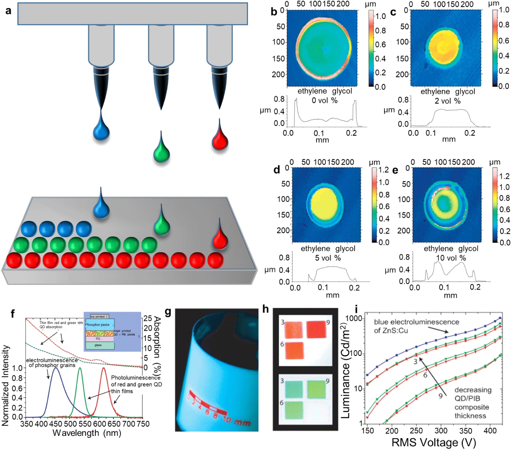
잉크 방울의 형성 후에는 잉크가 기판 위 증착되어 양자점 박막을 형성하는 과정에 대한 제어가 중요하다. 이 과정에서 흔히 발생하는 문제점 중 하나는 액상의 증발 과정에서 잉크의 중심보다 가장자리의 두께가 더 두꺼워져서 커피 얼룩과 같은 불균일한 두께의 패턴이 생기게 되는 현상인 ‘커피링 효과’이다[62-64]. 이를 해결하기 위해 유기첨가제를 사용하거나 용액의 조성을 제어하여 잉크의 증발과정을 제어하는 연구들이 이뤄지고 있다[65-66]. 대표적으로 CdTe 양자점을 이용한 잉크젯 인쇄 기술에 대한 초기 연구에서는 poly(vinylalcohol) 첨가제와 물과 에틸렌글리콜 용매의 조성제어를 통해 커피링 효과를 제어할 수 있음을 보여주었다(Fig. 4(b)Fig. 4(e))[67]. 1 wt%의 PVA가 첨가된 상황에서 에틸렌글리콜을 대략 2-5 vol% 첨가했을 때, 균일한 두께를 지니는 대략 130 μm 직경의 패턴이 형성되었다. 하지만, 에틸렌글리콜의 농도가 이보다 낮거나 높을 경우 불균일한 두께의 패턴이 형성됨을 확인할 수 있었다.

커피링 효과를 최소화하여 교류 구동 발광소자의 색변환층에 양자점을 적용하는 연구도 진행되었다(Fig. 4(f)Fig. 4(i))[68]. CdSe 기반의 코어/쉘 양자점 용액에 투명한 고분자인 polyisobutylene을 첨가하고, 헥산과 옥탄의 비율을 최적화하여 커피링 효과를 억제하고, 높은 균일성과 정확성으로 우수한 광특성을 지닌 양자점 패턴을 제작하였다. 유리기판뿐만 아니라, polyethylene terephthalate와 같은 유연기판에도 양자점이 잘 인쇄됨을 보여주었으며(Fig. 4(g)), 양자점 색변환층의 두께 최적화를 통해서 풀 컬러(full color) 디스플레이를 구현하였다(Fig. 4(h)Fig. 4(i)).

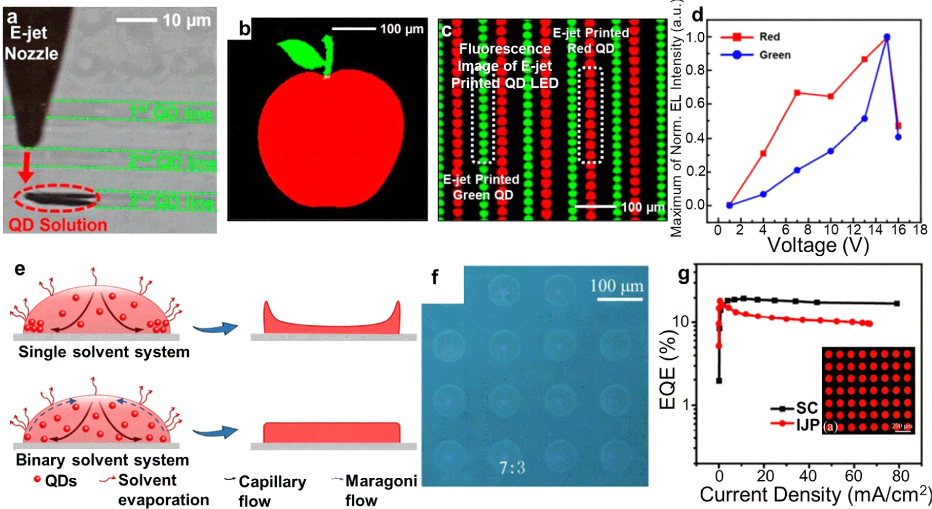
잉크젯 인쇄 기술을 이용하여 광발광 방식의 양자점 광학필름을 적용한 디스플레이를 넘어 양자점 전계발광소자에도 적용이 이루어지고 있다(Fig. 5(a)Fig. 5(d))[69]. 잉크의 조성, 노즐의 크기, 헤드의 속도, 전압 등의 요인들을 최적화하여 형성된 패턴의 두께에 대해 정밀한 제어와 고해상도 패터닝이 가능했다. 그 결과, 잉크젯 인쇄 공정을 통해 최대 외부양자효율 2.5%, 최대 휘도 36,000 cd/m2을 보이는 양자점 발광소자를 제작하였다(Fig. 5(d)). 최근에는 양자점 잉크젯 인쇄 기술을 적용하여 만들어진 양자점 발광소자의 성능 향상을 위한 지속적인 연구가 이루어지고 있다. 기존의 양자점 발광소자에서 poly(9,9-dioctylfluorene-co-N-(4-butylphenyl)diphenylamine, TFB)는 높은 이동도와 적절한 에너지 레벨로 정공수송층로 많이 활용되어져 왔다[70]. 하지만, 필름의 부식이나 낮은 표면에너지 등의 문제점으로 양자점 잉크젯 인쇄 기술을 적용시 TFB를 정공수송층으로 사용한 소자의 성능이 스핀코팅 방식으로 제작된 기존 양자점 발광소자에 비해 좋지 못하였다. 최근 이루어진 연구에서는 이성분계 양자점 잉크방식으로 해결할 수 있었다[71]. 용매로 높은 표면장력을 지니는 decalin을 사용하고, decalin과 n-tridecane의 비율을 최적화하여 TFB위에서도 고품질의 양자점 층을 인쇄하였다. 이를 통해 2,000 cd/m2에서 27시간의 긴 소자수명과 최대 외부양자효율 18.3%의 우수한 성능을 달성하였다.

jfpe-1-1-45-g5
Fig. 5. QLEDs fabricated by inkjet printing, (a) an optical microscope image of an nozzle and a printing substrate during E-jet printing, (b) fluorescence pattern images of red and green QDs printed in a raster scanning, (c) composite fluorescence images of E-jet printed QLED, (d) EL properties of E-jet printed QLED. Panels (a−d) were reprinted with permission from ref [69], Copyright 2015 American Chemical Society, (e) schematic illustration of the ink evaporation of single and binary solvent, (f) optical microscopic images of the films inkjet-printed onto TFB substrate with 7:3 volume ratio of decalin:n-tridecane solvent, (g) EQE-luminance property of inkjet-printed QLED. Panels (e−g) were reprinted with permission from ref [71]. Copyright 2021 Tsinghua University Press and Springer-Verlag GmbH Germany, part of Springer Nature.
Download Original Figure

4. TRANSFER PRINTING

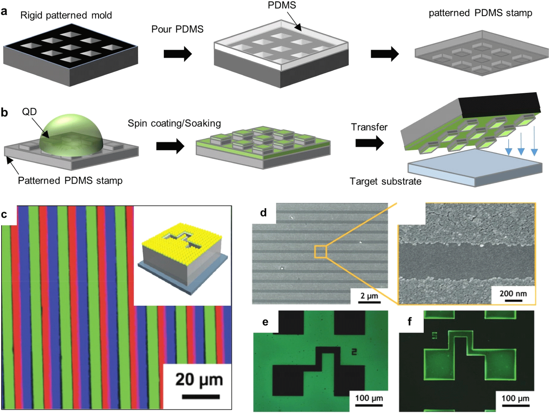
전사인쇄는 물리적인 접촉을 이용하여 대상 기판에 소재를 인쇄하는 기술로 주로 poly(dimethylsiloxane) (PDMS)와 같은 탄성중합체 스탬프를 사용하여 이루어진다[72-75]. 전통적인 전사인쇄법에서는 인쇄하고자 하는 패턴의 모양을 지닌 양각스탬프를 제조하여 사용하며(Fig. 6(a))[77,78] 전사 방식에 따라 적층전사인쇄(additive transfer printing)와 감산전사인쇄(subtractive transfer printing)로 나뉜다[79]. 적층전사인쇄는 패턴이 전사된 PDMS 양각스탬프에 양자점을 스핀코팅과 같은 코팅공정으로 고르게 코팅한 후 인쇄하는 방식이다(Fig. 6(b))[80-82]. 기판으로 사용되는 대부분의 재료들과 양자점 사이의 결합에너지가 PDMS와 양자점 사이의 결합에너지보다 크기 때문에 쉽게 기판으로의 전사가 가능하다[83]. 이 방식에서 perfluoropolyether와 같은 물질을 이용하여 스탬프의 강성을 제어하고, 표면을 불소 처리하여 표면에너지를 낮추어 더욱 안정적으로 전사를 할 수 있다(Fig. 6(c)Fig. 6(f))[84].

jfpe-1-1-45-g6
Fig. 6. Schematic illustration showing, (a) the stamp fabrication process and (b) the additive transfer printing, (c) fluorescence microscopy image of transferred RGB arrays, (d) scanning electron microscopy image of transferred QD arrays using a perfluoropolyether stamp, (e) fluorescence microscopy images of printed QDs and (f) QDs remained on the stamp after the transfer printing process. Panels (c−f) were reprinted with permission from ref 84. Copyright 2012 Wiley-VCH Verlag GmbH & Co. KGaA, Weinheim.
Download Original Figure

감산전사인쇄방식은 donor기판에 스핀코팅 방식으로 양자점을 도포해준 후, 양각의 PDMS 스탬프를 이용하여 최종 기판으로 양자점층을 전사한다(Fig. 7(a)) [85,86] 이때 donor 기판에 octadecyltrichlorosilane의 self-assembled monolayer 표면처리를 통해 기판의 표면에너지를 낮추어 양자점층의 박리를 용이하게 해서 대면적의 균일성을 향상시킬 수 있다[87]. 또한 donor 기판으로부터 양자점층을 박리할 때 높은 픽업수율을 위해서 스탬프의 적절한 박리 속도가 중요하기 때문에 이를 최적화하였다. 최종적으로 감산전사인쇄를 통해 풀 컬러 양자점 디스플레이를 구현하였다(Fig. 7(b)Fig.7(e)).

jfpe-1-1-45-g7
Fig. 7. Subtractive transfer printing of QDs, (a) schematic illustration of the subtractive transfer printing, (b) fluorescence image of the subtractive transferred RGB QD stripes, (c) scanning electron microscopy images comparing QD film morphology of a spin-coated QD film and a transfer-printed QD film, (d) electroluminescence properties of QLEDs fabricated by transfer printing and spin-coating, (e) flexible QLED patterned by transfer printing. Panels (b−e) were reprinted with permission from ref [85]. Copyright 2011 Springer Nature, (f) scanning electron microscopy image of the microholes of PDMS stamp, (g) fluorescence microscopy images of the QD films patterned by honeycomb holes, (h) schematic illustration and (i) EL properties of QLEDs with a honeycomb-shaped charge-blocking layer. Panels (f−i) were reprinted with permission from ref 88. Copyright 2022 Springer Nature.
Download Original Figure

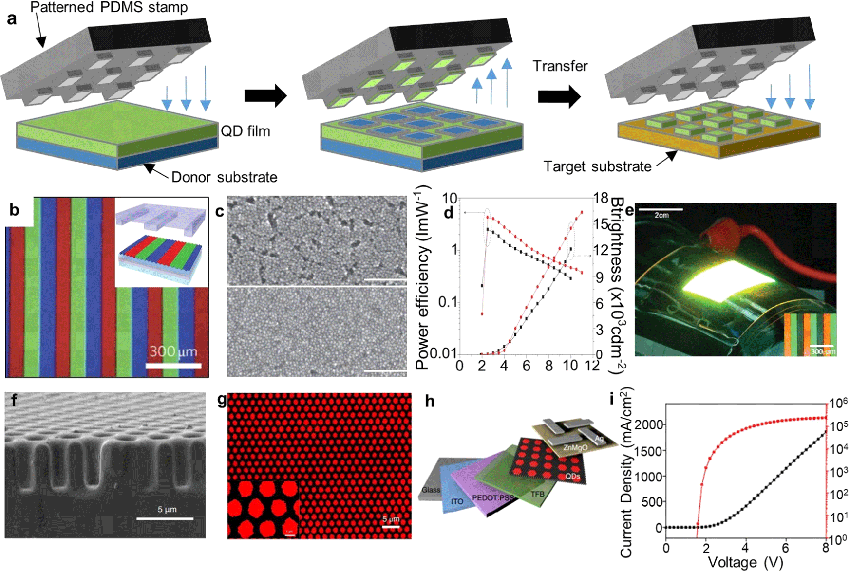
최근에는 Langmuir–Blodgett과 감산전사인쇄를 활용한 초고해상도 패터닝 연구가 보고되었다[88]. Langmuir–Blodgett공정으로 형성된 양자점 필름을 PDMS 스탬프를 통한 단층단위의 전사로 정밀한 두께제어가 가능하였으며, 전사필름의 균일성이 높여 25,400 pixel-per-inch(ppi)의 초고해상도 양자점 패터닝을 성취하였다. 또한 소자의 누설전류를 방지하기 위해 벌집모양의 전하 차단층을 패터닝하여 최고 외부양자효율 14.72%, 최대 휘도 262,400 cd/m2의 고성능의 양자점 발광소자를 제작하였다(Fig. 7(f)Fig. 7(i)).

앞서 설명했던 양각스탬프를 활용한 전통적인 전사인쇄기술과는 달리 음각스탬프를 활용하는 음각전사인쇄기술도 연구되어졌다[89]. 음각전사인쇄기술은 평평한 패턴이 없는 스탬프를 사용하며, 스탬프에 의해 픽업된 양자점층과 원하는 패턴과 역모양을 지닌 trench와의 접촉으로 전사하고자 하는 패턴을 제외한 나머지 양자점층이 trench에 남게 된다. 이후 원하는 기판에 전사하는 방식으로 공정이 진행된다(Fig. 8(a)).

jfpe-1-1-45-g8
Fig. 8. Intaglio transfer printing of QDs, (a) schematic illustration of the intaglio transfer printing of QDs, (b) comparison of the pattern shape acquired by the conventional transfer printing using structured stamps and the intaglio transfer printing, (c) fluorescence image of high-resolution RGB pixels, (d) comparison of transfer yield of the conventional transfer printing and the intaglio transfer printing for patterns with various line widths, (e) optical image of a flexible white QLED and (f) an electronic tattoo. Panels (b−f) were reprinted with permission from ref [89]. Copyright 2015 Springer Nature.
Download Original Figure

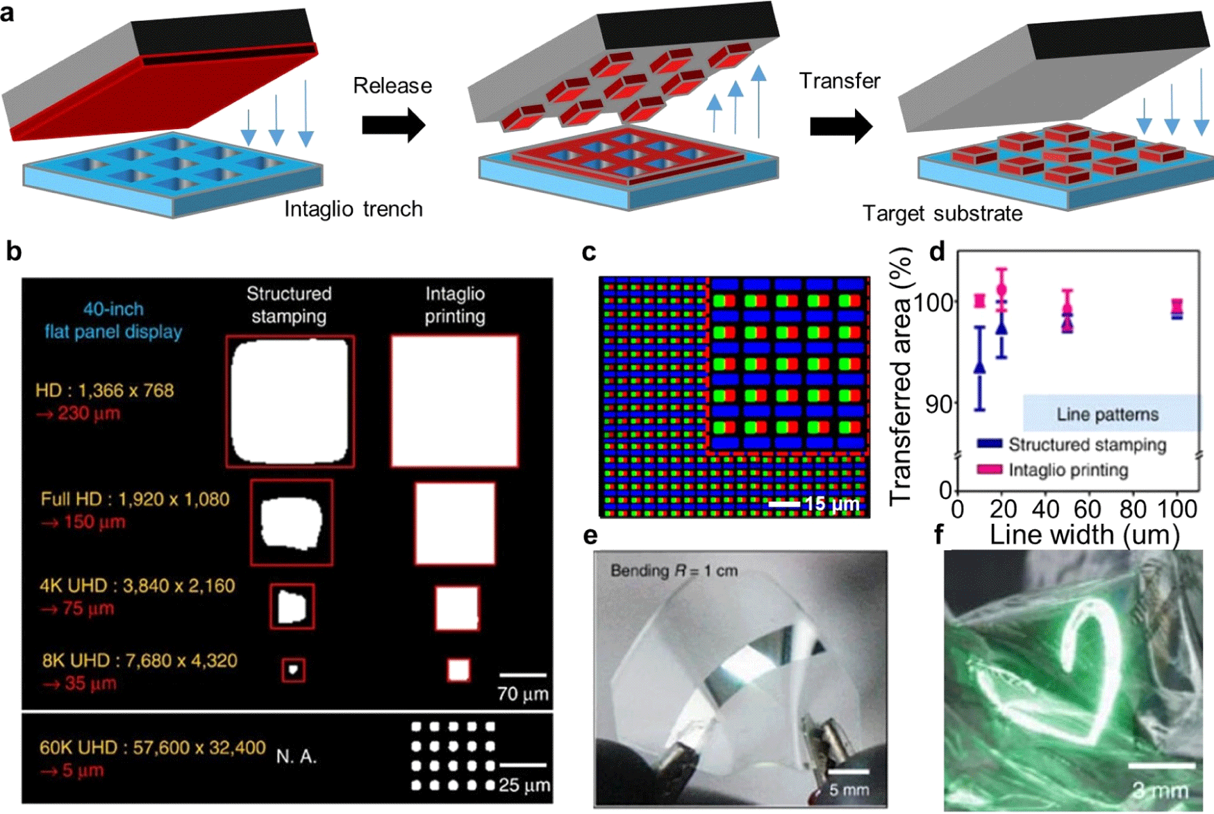
기존에는 양각스탬프에서는 전사하고자 하는 패턴의 크기가 작아질수록 전사과정에서 양각 패턴의 기계적 변형이 심해져 전사수율이 급격히 감소하지만, 음각전사인쇄기술에서는 작은 크기의 패턴에 대해서도 거의 100%의 전사수율을 보여줬다(Fig. 8(b)). 음각전사인쇄 방식을 통해서 2,460 ppi의 고해상도 RGB 픽셀 배열을 달성하였고, 이를 백색 발광소자와 14,000 cd/m2의 우수한 휘도를 나타내는 피부부착형 전자타투[90]에 적용하여 무궁무진한 응용가능성을 보여주었다(Fig. 8(c)Fig. 8(f)).

5. 결론 및 전망

본 종설논문에서는 발광소자 응용을 위한 콜로이드 양자점 인쇄공정 기술의 발전 동향에 대해서 논의하였다. 콜로이드 용액상에 분산되어 있는 양자점을 고체 형태의 양자점 필름으로 인쇄하는 기술은 양자점 발광소자와 같은 전자소자 구현을 위해 필수적이다. 또한, 입자의 크기나 모양, 구조뿐만 아니라, 주변 물질 및 양자점 입자 간의 상호작용에 의해서도 성질이 좌우되는 양자점의 특성상 각 인쇄공정의 기본적인 원리와 이에 따라 인쇄된 양자점에 미칠 수 있는 영향을 이해하는 것이 중요하다. 이를 통해 양자점의 특성 저하 및 서로 다른 색상의 양자점 간의 교차오염 없이 고해상도로 정확하게 양자점을 인쇄하는 기술이 필수적이다.

포토리소그래피, 잉크젯 프린팅, 전사인쇄 기술에 대해 집중적으로 논의하였으며, 각 기술들은 해상도 및 구현된 소자의 성능 면에서 많은 진보를 이루었지만, 여전히 기술적 개선이 필요한 상황이다. 대표적으로 포토리소그래피 공정 과정에서는 양자점의 변성 가능성이 존재하고, 잉크젯 공정에서는 마이크로미터 이하의 작은 패턴의 두께를 균일하게 제어하는 것이 어렵다. 또한, 이 두 가지 공정에서는 인쇄 후의 양자점 패턴에 남을 수 있는 유기 잔여물의 영향을 최소화하여야 한다. 한편, 물리적인 접촉을 통해 공정이 이루어지는 전사인쇄기술에서는 대면적 인쇄 기술 개발이 난제로 여겨지고 있다. 이외에도 지금까지 대부분의 양자점 인쇄기술들은 CdSe와 같이 중금속을 포함한 양자점을 기반으로 연구가 이뤄져왔기 때문에, 기술실용화를 위해서는 InP, ZnE, CuInE2 (E=S, Se, Te)와 같은 비중금속 양자점 기반의 패터닝 인쇄 기술에 대한 집중적인 연구가 필요하다[91-95]. 한편, 양자점 인쇄기술은 발광소자뿐만 아니라, 광센서[96,97] 태양전지[98] 광전기화학소자[99] 등의 다양한 양자점 소자들에 적용 가능하기 때문에 관련 기술 개발을 통해 양자점 기술 상용화에 큰 도움을 줄 수 있을 것으로 기대된다.

기호설명

HMDS:

Hexamethyldisilazane

PDMS:

Poly(dimethylsiloxane)

ppi:

Pixel-per-inch

QD:

Quantum dot

QLED:

Quantum dot light-emitting diode

RGB:

Red, green, and blue

TFB:

Poly(9,9-dioctylfluorene-co-N-(4-butylphenyl) diphenylamine

Funding

This work was supported by the DGIST R&D Program (21-HRHR-07) and the DGIST Start-up Fund Program (2022010026) of the Ministry of Science and ICT. This work was also supported by the National Research Foundation (NRF) grant funded by the Korea government (MSIT) (2021R1C1C1007844).

Declarations of Competing Interests

The authors declare that they have no competing interests.

REFERENCES

[1].

Woo, S. J.; Kim, J. S.; Lee, T. W. Characterization of Stability and Challenges to Improve Lifetime in Perovskite LEDs. Nat. Photonics 2021, 15 (9), 630-634.

[2].

Naresh, V.; Lee, N. Zn(II)-Doped Cesium Lead Halide Perovskite Nanocrystals with High Quantum Yield and Wide Color Tunability for Color-Conversion Light-Emitting Displays. ACS Appl. Nano Mater. 2020, 3 (8), 7621-7632.

[3].

Li, S.; Zhou, L.; Zhang, H. Investigation Progresses of Rare Earth Complexes as Emitters or Sensitizers in Organic Light-Emitting Diodes. Light Sci. Appl. 2022, 11 (1), 177.

[4].

Murray, C. B.; Norris, D. J.; Bawendi, M. G. Synthesis and Characterization of Nearly Monodisperse CdE (E=Sulfur, Selenium, Tellurium) Semiconductor Nanocrystallites. J. Am. Chem. Soc. 1993, 115 (19), 8706-8715.

[5].

Goesmann, H.; Feldmann, C. Nanoparticulate Functional Materials. Angew. Chem. 2010, 49 (8), 1362-1395.

[6].

Peng, X.; Manna, L.; Yang, W.; Wickham, J.; Scher, E.; Kadavanich, A.; Alivisatos, A. P. Shape Control of CdSe Nanocrystals. Nature. 2000, 404 (6773), 59-61.

[7].

Yang, J.; Son, J. S.; Yu, J. H.; Joo, J.; Hyeon, T. Advances in the Colloidal Synthesis of Two-Dimensional Semiconductor Nanoribbons. Chem. Mater. 2013, 25 (8), 1190-1198.

[8].

Yang, J.; Muckel, F.; Baek, W.; Fainblat, R.; Chang, H.; Bacher, G.; Hyeon, T. Chemical Synthesis, Doping, and Transformation of Magic-Sized Semiconductor Alloy Nanoclusters. J. Am. Chem. Soc. 2017, 139 (19), 6761-6770.

[9].

Colvin, V. L.; Schlamp, M. C.; Alivisatos, A. P. Light-Emitting Diodes Made from Cadmium Selenide Nanocrystals and a Semiconducting Polymer. Nature. 1994, 370 (6488), 354-357.

[10].

Shirasaki, Y.; Supran, G. J.; Bawendi, M. G.; Bulović, V. Emergence of Colloidal Quantum-Dot Light-Emitting Technologies. Nat. Photonics. 2013, 7(1), 13-23.

[11].

Dai, X.; Deng, Y.; Peng, X.; Jin, Y. Quantum-Dot Light-Emitting Diodes for Large-Area Displays: Towards the Dawn of Commercialization. Adv. Mater. 2017, 29 (14), 1607022.

[12].

Oh, N.; Kim, B. H.; Cho, S. Y.; Nam, S.; Rogers, S. P.; Jiang, Y.; Flanagan, J. C.; Zhai, Y.; Kim, J. H.; Lee, J.; Yu, Y.; Cho, Y. K.; Hur, G.; Zhang, J.; Trefonas, P.; Rogers, J. A.; Shim, M. Double-Heterojunction Nanorod Light-Responsive LEDs for Display Applications. Science 2017, 355 (6325), 616-619.

[13].

Yang, J.; Choi, M. K.; Yang, U. J.; Kim, S. Y.; Kim, Y. S.; Kim, J. H.; Kim, D. H.; Hyeon, T. Toward Full-Color Electroluminescent Quantum Dot Displays. Nano Lett. 2021, 21(1), 26-33.

[14].

Kim, D. C.; Yun, H.; Kim, J.; Seung, H.; Yu, W. S.; Koo, J. H.; Yang, J.; Kim, J. H.; Hyeon, T.; Kim, D. H. Three-Dimensional Foldable Quantum Dot Light-Emitting Diodes. Nat. Electron. 2021, 4(9), 671-680.

[15].

Choi, M. K.; Yang, J.; Hyeon, T.; Kim, D. H. Flexible Quantum Dot Light-Emitting Diodes for next-Generation Displays. npj. Flex. Electron. 2018, 2(1), 1-14.

[16].

Son, D.; Chae, S. I.; Kim, M.; Choi, M. K.; Yang, J.; Park, K.; Kale, V. S.; Koo, J. H.; Choi, C.; Lee, M.; Kim, J. H.; Hyeon, T.; Kim, D. H. Colloidal Synthesis of Uniform-Sized Molybdenum Disulfide Nanosheets for Wafer-Scale Flexible Nonvolatile Memory. Adv. Mater. 2016, 28 (42), 9326-9332.

[17].

Song, J. K.; Son, D.; Kim, J.; Yoo, Y. J.; Lee, G. J.; Wang, L.; Choi, M. K.; Yang, J.; Lee, M.; Do, K.; Koo, J. H.; Lu, N.; Kim, J. H.; Hyeon, T.; Song, Y. M.; Kim, D. H. Wearable Force Touch Sensor Array Using a Flexible and Transparent Electrode. Adv. Funct. Mater. 2017, 27 (6), 1605286.

[18].

Kim, J.; Shim, H. J.; Yang, J.; Choi, M. K.; Kim, D. C.; Kim, J.; Hyeon, T.; Kim, D. H. Ultrathin Quantum Dot Display Integrated with Wearable Electronics. Adv. Mater. 2017, 29 (38), 1700217.

[19].

Choi, M. K.; Yang, J.; Kim, D. C.; Dai, Z.; Kim, J.; Seung, H.; Kale, V. S.; Sung, S. J.; Park, C. R.; Lu, N.; Hyeon, T.; Kim, D. H. Extremely Vivid, Highly Transparent, and Ultrathin Quantum Dot Light-Emitting Diodes. Adv. Mater. 2018, 30 (1), 1703279.

[20].

Kim, T. H.; Lee, C. S.; Kim, S.; Hur, J.; Lee, S.; Shin, K. W.; Yoon, Y. Z.; Choi, M. K.; Yang, J.; Kim, D. H.; Hyeon, T.; Park, S.; Hwang, S. Fully Stretchable Optoelectronic Sensors Based on Colloidal Quantum Dots for Sensing Photoplethysmographic Signals. ACS Nano 2017, 11 (6), 5992-6003.

[21].

Lee, Y.; Kim, D. S.; Jin, S. W.; Lee, H.; Jeong, Y. R.; You, I.; Zi, G.; Ha, J. S. Stretchable Array of CdSe/ZnS Quantum-Dot Light Emitting Diodes for Visual Display of Bio-Signals. Chem. Eng. J. 2022, 427 (130858), 130858.

[22].

Yoo, J.; Li, S.; Kim, D. H.; Yang, J.; Choi, M. K. Materials and Design Strategies for Stretchable Electroluminescent Devices. Nanoscale Horiz 2022.

[23].

Kang, C. M.; Lee, H. Recent Progress of Organic Light-Emitting Diode Microdisplays for Augmented Reality/Virtual Reality Applications. J. Inf. Disp. 2022, 23 (1), 19-32.

[24].

Lee, T.; Kim, B. J.; Lee, H.; Hahm, D.; Bae, W. K.; Lim, J.; Kwak, J. Bright and Stable Quantum Dot Light-Emitting Diodes. Adv. Mater. 2022, 34 (4), e2106276.

[25].

Kim, T.; Kim, K. H.; Kim, S.; Choi, S. M.; Jang, H.; Seo, H. K.; Lee, H.; Chung, D. Y.; Jang, E. Efficient and Stable Blue Quantum Dot Light-Emitting Diode. Nature 2020, 586(7829), 385-389.

[26].

Won, Y. H.; Cho, O.; Kim, T.; Chung, D. Y.; Kim, T.; Chung, H.; Jang, H.; Lee, J.; Kim, D.; Jang, E. Highly Efficient and Stable InP/ZnSe/ZnS Quantum Dot Light-Emitting Diodes. Nature 2019, 575 (7784), 634-638.

[27].

Lee, S. H.; Song, S. W.; Yoon, S. Y.; Jo, D. Y.; Kim, S. K.; Kim, H. M.; Kim, Y.; Park, S. M.; Yang, H. Heterostructural Tailoring of Blue ZnSeTe Quantum Dots toward High-Color Purity and High-Efficiency Electroluminescence. Chem. Eng. J. 2022, 429 (132464), 132464.

[28].

Lee, J.; Yang, J.; Kwon, S. G.; Hyeon, T. Nonclassical Nucleation and Growth of Inorganic Nanoparticles. Nat. Rev. Mater. 2016, 1 (8), 1-16.

[29].

Yang, J.; Choi, M. K.; Kim, D. H.; Hyeon, T. Designed Assembly and Integration of Colloidal Nanocrystals for Device Applications. Adv. Mater. 2016, 28 (6), 1176-1207.

[30].

Kagan, C. R.; Lifshitz, E.; Sargent, E. H.; Talapin, D. V. Building Devices from Colloidal Quantum Dots. Science. 2016, 353 (6302), aac 5523-aac5523.

[31].

Yang, J.; Yoo, J.; Yu, W. S.; Choi, M. K. Polymer-Assisted High-Resolution Printing Techniques for Colloidal Quantum Dots. Macromol. Res. 2021, 29 (6), 391-401.

[32].

Sahu, N.; Parija, B.; Panigrahi, S. Fundamental Understanding and Modeling of Spin Coating Process: A Review. Indian J. Phys. Proc. Indian Assoc. Cultiv. Sci.(2004) 2009, 83 (4), 493-502.

[33].

Yang, M.; Chang, C.; Zhang, W.; Liu, Z.; Zhang, Q. Effect of Solvents of Quantum Dots on QLED Performance. IOP Conf. Ser. Mater. Sci. Eng. 2019, 562 (1), 012083.

[34].

Nam, T. W.; Kim, M.; Wang, Y.; Kim, G. Y.; Choi, W.; Lim, H.; Song, K. M.; Choi, M. J.; Jeon, D. Y.; Grossman, J. C.; Jung, Y. S. Thermodynamic-Driven Polychromatic Quantum Dot Patterning for Light-Emitting Diodes beyond Eye-Limiting Resolution. Nat. Commun. 2020, 11 (1), 3040.

[35].

Hong, A.; Kim, J.; Kwak, J. Sunlike White Quantum Dot Light-emitting Diodes with High Color Rendition Quality. Adv. Opt. Mater. 2020, 8 (22), 2001051.

[36].

Park, J.; Seung, H.; Kim, D. C.; Kim, M. S.; Kim, D. H. Unconventional Image-sensing and Light-emitting Devices for Extended Reality. Adv. Funct. Mater. 2021, 31( 39), 2009281.

[37].

Myeong, S.; Chon, B.; Kumar, S.; Son, H. J.; Kang, S. O.; Seo, S. Quantum Dot Photolithography Using a Quantum Dot Photoresist Composed of an Organic-Inorganic Hybrid Coating Layer. Nanoscale Adv. 2022, 4 (4), 1080-1087.

[38].

Bertino, M. F.; Gadipalli, R. R.; Martin, L. A.; Rich, L. E.; Yamilov, A.; Heckman, B. R.; Leventis, N.; Guha, S.; Katsoudas, J.; Divan, R.; Mancini, D. C. Quantum Dots by Ultraviolet and X-Ray Lithography. Nanotechnology. 2007, 18 (31), 315603.

[39].

Kim, G. H.; Lee, J.; Lee, J. Y.; Han, J.; Choi, Y.; Kang, C. J.; Kim, K. B.; Lee, W.; Lim, J.; Cho, S. Y. High-Resolution Colloidal Quantum Dot Film Photolithography via Atomic Layer Deposition of ZnO. ACS Appl. Mater. Interfaces 2021, 13 (36), 43075-43084.

[40].

Kim, Y. H.; Koh, S.; Lee, H.; Kang, S. M.; Lee, D. C.; Bae, B. S. Photo-Patternable Quantum Dots/Siloxane Composite with Long-Term Stability for Quantum Dot Color Filters. ACS Appl. Mater. Interfaces 2020, 12 (3), 3961-3968.

[41].

Bae, W. K.; Kwak, J.; Lim, J.; Lee, D.; Nam, M. K.; Char, K.; Lee, C.; Lee, S. Multicolored Light-Emitting Diodes Based on All-Quantum-Dot Multilayer Films Using Layer-by-Layer Assembly Method. Nano Lett. 2010, 10 (7), 2368-2373.

[42].

Park, J. S.; Kyhm, J.; Kim, H. H.; Jeong, S.; Kang, J.; Lee, S. E.; Lee, K. T.; Park, K.; Barange, N.; Han, J.; Song, J. D.; Choi, W. K.; Han, I. K. Alternative Patterning Process for Realization of Large-Area, Full-Color, Active Quantum Dot Display. Nano Lett. 2016, 16 (11), 6946-6953.

[43].

Mei, W.; Zhang, Z.; Zhang, A.; Li, D.; Zhang, X.; Wang, H.; Chen, Z.; Li, Y.; Li, X.; Xu, X. High-Resolution, Full-Color Quantum Dot Light-Emitting Diode Display Fabricated via Photolithography Approach. Nano Res. 2020, 13 (9), 2485-2491.

[44].

Ji, T.; Jin, S.; Zhang, H.; Chen, S.; Sun, X. W. Full Color Quantum Dot Light-Emitting Diodes Patterned by Photolithography Technology: QLEDs Patterned by Photolithography Technology. J. Soc. Inf. Disp. 2018, 26 (3), 121-127.

[45].

Wang, Y.; Fedin, I.; Zhang, H.; Talapin, D. V. Direct Optical Lithography of Functional Inorganic Nanomaterials. Science 2017, 357 (6349), 385-388.

[46].

Cho, H.; Pan, J. A.; Wu, H.; Lan, X.; Coropceanu, I.; Wang, Y.; Cho, W.; Hill, E. A.; Anderson, J. S.; Talapin, D. V. Direct Optical Patterning of Quantum Dot Light-Emitting Diodes via In Situ Ligand Exchange. Adv. Mater. 2020, 32 (46), e2003805.

[47].

Yang, J.; Hahm, D.; Kim, K.; Rhee, S.; Lee, M.; Kim, S.; Chang, J. H.; Park, H. W.; Lim, J.; Lee, M.; Kim, H.; Bang, J.; Ahn, H.; Cho, J. H.; Kwak, J.; Kim, B.; Lee, C.; Bae, W. K.; Kang, M. S. High-Resolution Patterning of Colloidal Quantum Dots via Non-Destructive, Light-Driven Ligand Crosslinking. Nat. Commun. 2020, 11 (1), 2874.

[48].

van Osch, T. H. J.; Perelaer, J.; de Laat, A. W. M.; Schubert, U. S. Inkjet Printing of Narrow Conductive Tracks on Untreated Polymeric Substrates. Adv. Mater. 2008, 20 (2), 343-345.

[49].

Xing, Z.; Zhuang, J.; Wei, C.; Zhang, D.; Xie, Z.; Xu, X.; Ji, S.; Tang, J.; Su, W.; Cui, Z. Inkjet-Printed Quantum Dot Light-Emitting Diodes with an Air-Stable Hole Transport Material. ACS Appl. Mater. Interfaces. 2017, 9 (19), 16351-16359.

[50].

Bao, B.; Li, M.; Li, Y.; Jiang, J.; Gu, Z.; Zhang, X.; Jiang, L.; Song, Y. Patterning Fluorescent Quantum Dot Nanocomposites by Reactive Inkjet Printing. Small. 2015, 11 (14), 1649-1654.

[51].

Sliz, R.; Lejay, M.; Fan, J. Z.; Choi, M. J.; Kinge, S.; Hoogland, S.; Fabritius, T.; García de Arquer, F. P.; Sargent, E. H. Stable Colloidal Quantum Dot Inks Enable Inkjet-Printed High-Sensitivity Infrared Photodetectors. ACS Nano. 2019, 13 (10), 11988-11995.

[52].

Ho, S. J.; Hsu, H. C.; Yeh, C. W.; Chen, H. S. Inkjet-Printed Salt-Encapsulated Quantum Dot Film for UV-Based RGB Color-Converted Micro-Light Emitting Diode Displays. ACS Appl. Mater. Interfaces 2020, 12 (29), 33346-33351.

[53].

Singh, M.; Haverinen, H. M.; Dhagat, P.; Jabbour, G. E. Inkjet Printing-Process and Its Applications. Adv. Mater. 2010, 22 (6), 673-685.

[54].

Jun, H. Y.; Ryu, S. O.; Kim, S. H.; Kim, J. Y.; Chang, C. H.; Ryu, S. O.; Choi, C. H. Inkjet Printing of Few-layer Enriched Black Phosphorus Nanosheets for Electronic Devices. Adv. Electron. Mater. 2021, 7 (10), 2100577.

[55].

Haverinen, H. M.; Myllylä, R. A.; Jabbour, G. E. Inkjet Printing of Light Emitting Quantum Dots. Appl. Phys. Lett. 2009, 94 (7), 073108.

[56].

Service, R. F. Materials Research Society Meeting. Printable Electronics That Stick Around. Science 2004, 304 (5671), 675.

[57].

Gao, M.; Li, L.; Song, Y. Inkjet Printing Wearable Electronic Devices. J. Mater. Chem. C Mater. Opt. Electron. Devices 2017, 5 (12), 2971-2993.

[58].

Derby, B. Additive Manufacture of Ceramics Components by Inkjet Printing. Engineering (Beijing) 2015, 1 (1), 113-123.

[59].

Wijshoff, H. Drop Dynamics in the Inkjet Printing Process. Curr. Opin. Colloid Interface Sci. 2018, 36, 20-27.

[60].

Jia, S.; Tang, H.; Ma, J.; Ding, S.; Qu, X.; Xu, B.; Wu, Z.; Li, G.; Liu, P.; Wang, K.; Sun, X. W. High Performance Inkjet-printed Quantum-dot Light-emitting Diodes with High Operational Stability. Adv. Opt. Mater. 2021, 9 (22), 2101069.

[61].

Liu, Y.; Derby, B. Experimental Study of the Parameters for Stable Drop-on-Demand Inkjet Performance. Phys. Fluids 2019, 31 (3), 032004.

[62].

Lohse, D. Fundamental Fluid Dynamics Challenges in Inkjet Printing. Annu. Rev. Fluid Mech. 2022, 54 (1), 349-382.

[63].

Mampallil, D.; Eral, H. B. A Review on Suppression and Utilization of the Coffee-Ring Effect. Adv. Colloid Interface Sci. 2018, 252, 38-54.

[64].

Zhang, Z.; Zhang, X.; Xin, Z.; Deng, M.; Wen, Y.; Song, Y. Controlled Inkjetting of a Conductive Pattern of Silver Nanoparticles Based on the Coffee-Ring Effect. Adv. Mater. 2013, 25 (46), 6714-6718.

[65].

Hu, H.; Larson, R. G. Marangoni Effect Reverses Coffee-Ring Depositions. J. Phys. Chem. B 2006, 110 (14), 7090-7094.

[66].

Jiang, C.; Zhong, Z.; Liu, B.; He, Z.; Zou, J.; Wang, L.; Wang, J.; Peng, J.; Cao, Y. Coffee-Ring-Free Quantum Dot Thin Film Using Inkjet Printing from a Mixed-Solvent System on Modified ZnO Transport Layer for Light-Emitting Devices. ACS Appl. Mater. Interfaces 2016, 8 (39), 26162-26168.

[67].

Tekin, E.; Smith, P. J.; Hoeppener, S.; van den Berg, A. M. J.; Susha, A. S.; Rogach, A. L.; Feldmann, J.; Schubert, U. S. Inkjet Printing of Luminescent CdTe Nanocrystal-Polymer Composites. Adv. Funct. Mater. 2007, 17 (1), 23-28.

[68].

Wood, V.; Panzer, M. J.; Chen, J.; Bradley, M. S.; Halpert, J. E.; Bawendi, M. G.; Bulović, V. Inkjet-Printed Quantum Dot-Polymer Composites for Full-Color AC-Driven Displays. Adv. Mater. 2009, 21 (21), 2151-2155.

[69].

Kim, B. H.; Onses, M. S.; Lim, J. B.; Nam, S.; Oh, N.; Kim, H.; Yu, K. J.; Lee, J. W.; Kim, J. H.; Kang, S. K.; Lee, C. H.; Lee, J.; Shin, J. H.; Kim, N. H.; Leal, C.; Shim, M.; Rogers, J. A. High-Resolution Patterns of Quantum Dots Formed by Electrohydrodynamic Jet Printing for Light-Emitting Diodes. Nano Lett. 2015, 15 (2), 969-973.

[70].

Yang, Y.; Zheng, Y.; Cao, W.; Titov, A.; Hyvonen, J.; Manders, J. R.; Xue, J.; Holloway, P. H.; Qian, L. High-Efficiency Light-Emitting Devices Based on Quantum Dots with Tailored Nanostructures. Nat. Photonics 2015, 9 (4), 259-266.

[71].

Chen, M.; Xie, L.; Wei, C.; Yi, Y. Q. Q.; Chen, X.; Yang, J.; Zhuang, J.; Li, F.; Su, W.; Cui, Z. High Performance Inkjet-Printed QLEDs with 18.3% EQE: Improving Interfacial Contact by Novel Halogen-Free Binary Solvent System. Nano Res. 2021, 14 (11), 4125-4131.

[72].

Meitl, M. A.; Zhu, Z. T.; Kumar, V.; Lee, K. J.; Feng, X.; Huang, Y. Y.; Adesida, I.; Nuzzo, R. G.; Rogers, J. A. Transfer Printing by Kinetic Control of Adhesion to an Elastomeric Stamp. Nat. Mater. 2006, 5 (1), 33-38.

[73].

Zhou, H.; Qin, W.; Yu, Q.; Cheng, H.; Yu, X.; Wu, H. Transfer Printing and Its Applications in Flexible Electronic Devices. Nanomaterials (Basel) 2019, 9 (2), 283.

[74].

Liu, X.; Cao, Y.; Zheng, K.; Zhang, Y.; Wang, Z.; Chen, Y.; Chen, Y.; Ma, Y.; Feng, X. Liquid Droplet Stamp Transfer Printing. Adv. Funct. Mater. 2021, 31 (52), 2105407.

[75].

Yang, J.; Choi, M. K.; Sheng, Y.; Jung, J.; Bustillo, K.; Chen, T.; Lee, S. W.; Ercius, P.; Kim, J. H.; Warner, J. H.; Chan, E. M.; Zheng, H. MoS2 Liquid Cell Electron Microscopy through Clean and Fast Polymer-Free MoS2 Transfer. Nano Lett. 2019, 19 (3), 1788-1795.

[76].

Choi, M. K.; Park, I.; Kim, D. C.; Joh, E.; Park, O. K.; Kim, J.; Kim, M.; Choi, C.; Yang, J.; Cho, K. W.; Hwang, J. H.; Nam, J. M.; Hyeon, T.; Kim, J. H.; Kim, D. H. Thermally Controlled, Patterned Graphene Transfer Printing for Transparent and Wearable Electronic/Optoelectronic System. Adv. Funct. Mater. 2015, 25 (46), 7109-7118.

[77].

Hines, D. R.; Ballarotto, V. W.; Williams, E. D.; Shao, Y.; Solin, S. A. Transfer Printing Methods for the Fabrication of Flexible Organic Electronics. J. Appl. Phys. 2007, 101 (2), 024503.

[78].

Joo, C. W.; Jeon, S. O.; Yook, K. S.; Lee, J. Y. Improved Device Performances in Polymer Light-Emitting Diodes Using a Stamp Transfer Printing Process. Org. Electron. 2009, 10 (2), 372-375.

[79].

Liao, W. S.; Cheunkar, S.; Cao, H. H.; Bednar, H. R.; Weiss, P. S.; Andrews, A. M. Subtractive Patterning via Chemical Lift-off Lithography. Science 2012, 337 (6101), 1517-1521.

[80].

Kim, L.; Anikeeva, P. O.; Coe-Sullivan, S. A.; Steckel, J. S.; Bawendi, M. G.; Bulović, V. Contact Printing of Quantum Dot Light-Emitting Devices. Nano Lett. 2008, 8 (12), 4513-4517.

[81].

Carlson, A.; Bowen, A. M.; Huang, Y.; Nuzzo, R. G.; Rogers, J. A. Transfer Printing Techniques for Materials Assembly and Micro/Nanodevice Fabrication. Adv. Mater. 2012, 24 (39), 5284-5318.

[82].

Joo, S.; Lee, C. E.; Kang, J.; Seo, S.; Song, Y. K.; Kim, J. H. Intaglio Contact Printing of Versatile Carbon Nanotube Composites and Its Applications for Miniaturizing High-Performance Devices. Small 2022, 18 (3), e2106174.

[83].

Xue, M.; Zhang, Z.; Zhu, N.; Wang, F.; Zhao, X. S.; Cao, T. Transfer Printing of Metal Nanoparticles with Controllable Dimensions, Placement, and Reproducible Surface-Enhanced Raman Scattering Effects. Langmuir 2009, 25 (8), 4347-4351.

[84].

Sung, S. H.; Yoon, H.; Lim, J.; Char, K. Reusable Stamps for Printing Sub-100 Nm Patterns of Functional Nanoparticles. Small 2012, 8 (6), 826-831.

[85].

Kim, T. H.; Cho, K. S.; Lee, E. K.; Lee, S. J.; Chae, J.; Kim, J. W.; Kim, D. H.; Kwon, J. Y.; Amaratunga, G.; Lee, S. Y.; Choi, B. L.; Kuk, Y.; Kim, J. M.; Kim, K. Full-Colour Quantum Dot Displays Fabricated by Transfer Printing. Nat. Photonics 2011, 5 (3), 176-182.

[86].

Kim, T. H.; Chung, D. Y.; Ku, J.; Song, I.; Sul, S.; Kim, D. H.; Cho, K. S.; Choi, B. L.; Kim, J. M.; Hwang, S.; Kim, K. Heterogeneous Stacking of Nanodot Monolayers by Dry Pick-and-Place Transfer and Its Applications in Quantum Dot Light-Emitting Diodes. Nat. Commun. 2013, 4 (1), 2637.

[87].

Kim, B. H.; Nam, S.; Oh, N.; Cho, S. Y.; Yu, K. J.; Lee, C. H.; Zhang, J.; Deshpande, K.; Trefonas, P.; Kim, J. H.; Lee, J.; Shin, J. H.; Yu, Y.; Lim, J. B.; Won, S. M.; Cho, Y. K.; Kim, N. H.; Seo, K. J.; Lee, H.; Kim, T. I.; Shim, M.; Rogers, J. A. Multilayer Transfer Printing for Pixelated, Multicolor Quantum Dot Light-Emitting Diodes. ACS Nano 2016, 10 (5), 4920-4925.

[88].

Meng, T.; Zheng, Y.; Zhao, D.; Hu, H.; Zhu, Y.; Xu, Z.; Ju, S.; Jing, J.; Chen, X.; Gao, H.; Yang, K.; Guo, T.; Li, F.; Fan, J.; Qian, L. Ultrahigh-Resolution Quantum-Dot Light-Emitting Diodes. Nat. Photonics 2022, 16 (4), 297-303.

[89].

Choi, M. K.; Yang, J.; Kang, K.; Kim, D. C.; Choi, C.; Park, C.; Kim, S. J.; Chae, S. I.; Kim, T. H.; Kim, J. H.; Hyeon, T.; Kim, D. H. Wearable Red-Green-Blue Quantum Dot Light-Emitting Diode Array Using High-Resolution Intaglio Transfer Printing. Nat. Commun. 2015, 6 (1), 7149.

[90].

Yang, J. C.; Mun, J.; Kwon, S. Y.; Park, S.; Bao, Z.; Park, S. Electronic Skin: Recent Progress and Future Prospects for Skin-Attachable Devices for Health Monitoring, Robotics, and Prosthetics. Adv. Mater. 2019, 31 (48), e1904765.

[91].

Yang, J.; Kim, J. Y.; Yu, J. H.; Ahn, T. Y.; Lee, H.; Choi, T. S.; Kim, Y. W.; Joo, J.; Ko, M. J.; Hyeon, T. Copper-Indium-Selenide Quantum Dot-Sensitized Solar Cells. Phys. Chem. Chem. Phys. 2013, 15 (47), 20517-20525.

[92].

Yu, J. H.; Kim, J.; Hyeon, T.; Yang, J. Facile Synthesis of Manganese(II)-Doped ZnSe Nanocrystals with Controlled Dimensionality. J. Chem. Phys. 2019, 151 (24), 244701.

[93].

Chen, B.; Li, D.; Wang, F. InP Quantum Dots: Synthesis and Lighting Applications. Small 2020, 16 (32), e2002454.

[94].

Roh, H.; Ko, D.; Shin, D. Y.; Chang, J. H.; Hahm, D.; Bae, W. K.; Lee, C.; Kim, J. Y.; Kwak, J. Enhanced Performance of Pixelated Quantum Dot Light-emitting Diodes by Inkjet Printing of Quantum Dot-Polymer Composites. Adv. Opt. Mater. 2021, 9 (11), 2002129.

[95].

Tian, W.; Dou, L.; Jin, Z.; Xiao, J.; Li, J. Full-Color Micro-LED Displays with Cadmium-Free Quantum Dots Patterned by Photolithography Technology. Appl. Opt. 2020, 59 (35), 11112-11122.

[96].

Zhou, W.; Zheng, L.; Ning, Z.; Cheng, X.; Wang, F.; Xu, K.; Xu, R.; Liu, Z.; Luo, M.; Hu, W.; Guo, H.; Zhou, W.; Yu, Y. Silicon: Quantum Dot Photovoltage Triodes. Nat. Commun. 2021, 12 (1), 6696.

[97].

Kim, J.; Kwon, S. M.; Kang, Y. K.; Kim, Y. H.; Lee, M. J.; Han, K.; Facchetti, A.; Kim, M. G.; Park, S. K. A Skin-like Two-Dimensionally Pixelized Full-Color Quantum Dot Photodetector. Sci. Adv. 2019, 5 (11), eaax8801.

[98].

Kim, J. Y.; Yang, J.; Yu, J. H.; Baek, W.; Lee, C. H.; Son, H. J.; Hyeon, T.; Ko, M. J. Highly Efficient Copper-Indium-Selenide Quantum Dot Solar Cells: Suppression of Carrier Recombination by Controlled ZnS Overlayers. ACS Nano 2015, 9 (11), 11286-11295.

[99].

Kim, H. E.; Kim, J.; Ra, E. C.; Zhang, H.; Jang, Y. J.; Lee, J. S. Photoelectrochemical Nitrate Reduction to Ammonia on Ordered Silicon Nanowire Array Photocathodes. Angew. Chem. 2022, 61 (25), e202204117.

AUTHORS

송현화

jfpe-1-1-45-i1

2016년~2022년 : 충남대학교 신소재공학과 학사

2022년~현재: DGIST 에너지공학과 석사과정

[관심분야] 양자점 합성, 양자점 발광소자, 양자점 인쇄기술, 웨어러블 디스플레이

양지웅

jfpe-1-1-45-i2

2007년~2011년: 서울대학교 화학생물공학부 학사

2011년~2016년: 서울대학교 화학생물공학부 박사

2017년~2019년: 로렌스 버클리 국립연구소 박사후연구원

2019년~현재: DGIST 에너지공학과 조교수

[관심분야] 나노소재 합성화학, 양자점 광전자소자, 광촉매, 전자현미경