
1. INTRODUCTION
Printing technology is considered as one of the most promising methods for realizing low-cost and low-temperature electronic components such as thin-film transistors (TFTs), sensors, microelectromechanical systems (MEMS), and radio-frequency identification tags on large-area platforms [1-13]. Among these applications, inkjet-printed microelectromechanical (MEM) relay with movable cantilevers operated by electrostatic actuation has attracted significant interest as an ideal switching device that can substitute conventional TFTs due to its extremely low-leakage current, excellent environmental stability, subthreshold swing (SS), and an on/off ratio although printed TFTs have shown drastically improved electrical characteristics in the past decades [11-16]. Specifically, inkjet printing allows the controllable mechanical stiffness of a floated beam by exploiting the coffee-ring effect offering much enhanced stiffness and durability. Moreover, as an inkjet-printed 4-terminal (4T) MEM relay and inverter using a nanoparticle-type silver ink were reported, the printed relays can now offer low-power consumption complementary logic for systems exhibiting sharp transition characteristics [16]. In the design of integrated systems with the relay, one of the essential requirements is thermal and mechanical reliability because they limit the electrical performance during the operation by influencing the effective actuation gap and effective spring constant [17]. Although 2- and 3-terminal MEM switches were presented showing a low-switching voltage and high-frequency operation, further improvements on the maximum number of the operating cycles (< 200) are necessary for practical applications [18,19]. Therefore, although the failure mechanisms have been widely investigated, they have been limited to conventional silicon-based MEM switches having more robust movable parts and smaller contact gaps [20-22].
For inkjet-printed MEM relays using nanoparticle-type inks, electrical and mechanical reliabilities are an even more critical aspect than in the case of conventional silicon-MEM/nanoelectromechanical (NEM) relays because printed MEM relays have extremely low contact resistance below 10 Ω, resulting in a high current density and excess heat-generation on the contact region due to Joule heating [12-14]. The generated heat can aggravate welding, electromigration, surface oxidation of the contact region between the drain and source beams. These phenomena degrade the stiffness of the beam, restoring force, and on-current, respectively. Since the floated movable part in the relays is actuated by electrostatic force, the electrical characteristics, especially pull-in voltage (VPI) and mechanical delay, are also significantly sensitive to an actuation gap and a charging on the gate dielectric. In addition, since the suggested inkjet-printed 4T MEM relay has two movable beams bonded by an epoxy layer, mechanical strain distribution during the movable part's downward travel should be investigated since it may accelerate collapse-related issues or break down of the beams [16]. Therefore, it is critical to determine what failure mechanism is the most important to the inkjet-printed 4T MEM relay.
In this work, we report the mechanical and electrical reliability of an inkjet-printed 4T MEM relay in various failure modes: mechanical fatigue, welding at contact regions between the movable beam and the bottom electrode, charging on the gate dielectric, and surface oxidation of the contacting area. The MEM relays were operated with various bias conditions to measure the maximum number of endurance cycles and current flow capacity, which is a critical origin of the thermal stress by Joule heating. Effects of dielectric charging and surface oxidation during the operation were also investigated by measuring a change of the VPI and drain-source current (IDS), respectively. From these experiments, it was determined that welding-induced failures were dominant in limiting the maximum endurance cycles of the inkjet-printed MEM relays because of an extremely low metallic contact resistance (~4 Ω) resulting in high on-state current density.
2. METHODS
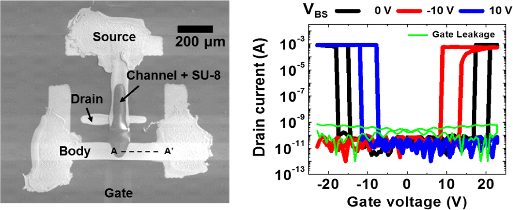
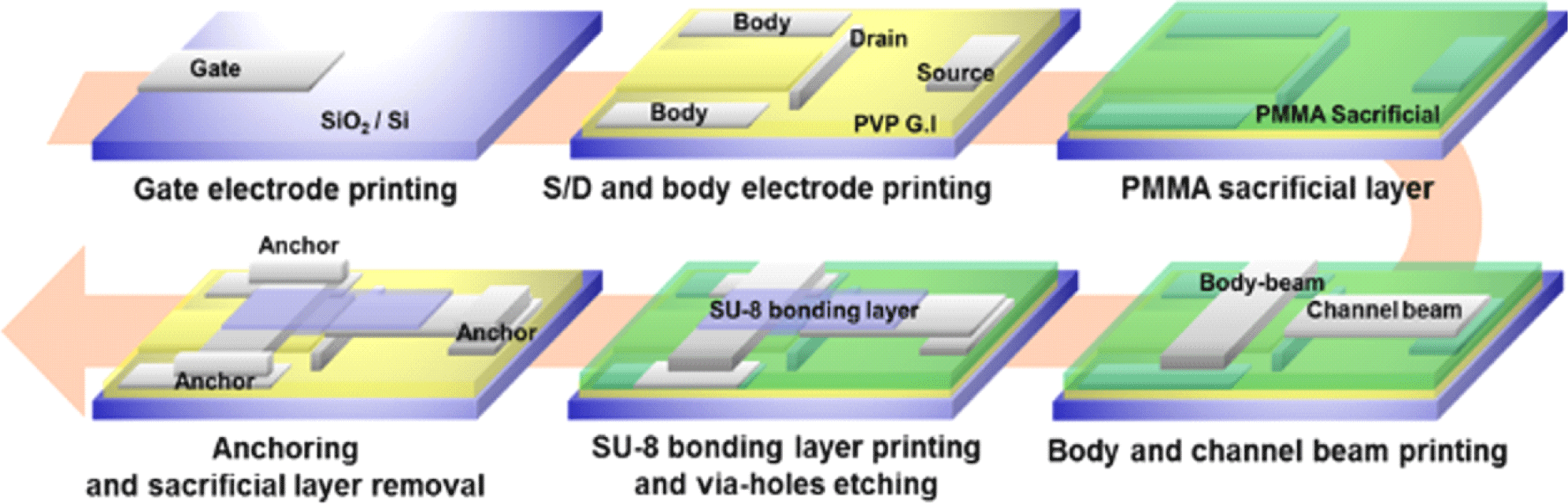
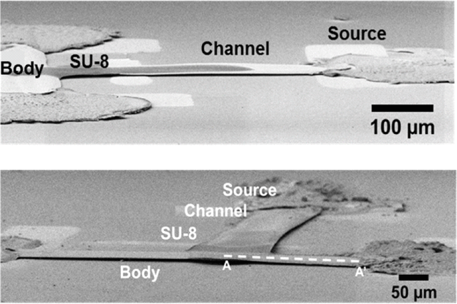
Fig. 1 shows the fabrication process flow of the inkjet-printed 4T MEM relay. Onto a cleaned silicon wafer with a thermally grown oxide layer (100 nm), the gate electrode was inkjet-printed using a commercial nanoparticle-based silver ink (EMD 6503 from Sunchemical Corp.). It was then sintered at 180°C on a hot plate for 30 min. The film thickness and sheet resistance of the electrode were 400 nm and 0.6 Ω/sq, respectively. To prevent a contact between the gate and floated beams caused by an excessive electrostatic force, a poly-4 (vinylphenol) (PVP) solution composed of 10 wt% PVP and 2 wt% poly (melamine-coformaldehyde), used as a cross-linking agent, were dissolved in propylene glycol methyl ether acetate and spin-coated onto the printed gate electrodes. The dielectric was dried and cross-linked for 10 min and 30 min on a 100°C and 200°C hot plate, respectively. The source/drain (S/D) and body-anchor electrodes were also inkjet-printed using the same silver ink used for the gate electrode, and then thermally sintered at 180°C on a hot plate for 30 min. Note that the drain electrode was printed in 3 passes on a 60°C substrate to create a high ridge at both edges. This approach allows a small contact area and contact gap, resulting in a narrower hysteresis window and lower VPI, respectively. After forming polymethyl (methacrylate) (PMMA, A11 from MicroChem Corp.) sacrificial layer (film thickness ~1.55 μm), the body and channel beams were printed orthogonally in seven passes on a 60°C substrate using the same silver ink used for the bottom electrodes without any surface treatment or interspersed drying process, providing an equivalent thickness of 2.5 μm. The printed beams were carefully sintered at a ramping condition of 2°C/min up to 180°C to yield a well-deposited, thick film without cracks. The two beams were separated by a spacing of ~100 μm to prevent leakage, were bonded together by an inkjet-printed SU-8 2002 layer (MicroChem), and then were fully cured on a 95°C hot plate for 1 min with UVO exposure for 30 s, then on a 95°C hot plate for 2 min, sequentially. The bonding bridge was printed in two passes to provide a sufficient thickness yielding the strongly suspended movable part. To define the anchor region, acetone printing was conducted to form holes through the PMMA sacrificial layer. Then, the beams and underlying anchor pads were anchored by filling the Ag ink through the etched via-hole. The resulting Ag posts were dried on a 125°C hot plate for 30 min and then sintered with a ramp condition of 5°C/min up to 180°C to minimize thermal damage to the weakened sacrificial layer. Finally, the PMMA sacrificial layer was removed by dipping into boiling acetone and isopropyl alcohol (IPA) sequentially, and then dried on a 150°C hot plate. The fabrication processes were executed in air at a maximum temperature of 200 °C. The electrical properties of the printed MEM relay were measured using a semiconductor parameter analyzer (4155C, Agilent Technologies) in air. The thicknesses and surface profiles of the printed components were measured using a surface profilometer (Dektak 6M, Veeco) and a white-light interferometer system (Wyko NT3300, Veeco). The scanning electron microscope (SEM) images were obtained with an FEI Nova NanoSEM 650. The mechanical stiffnesses of the cantilever beam and the printed silver electrodes were measured using a TI 900 TriboIndenter nanoindenter. The fabricated 4T MEM relay was well-floated with the strongly suspended movable part maintaining a constant actuation gap without any curling- or collapse-related failure, as shown in Fig. 2.
3. RESULTS AND DISCUSSION
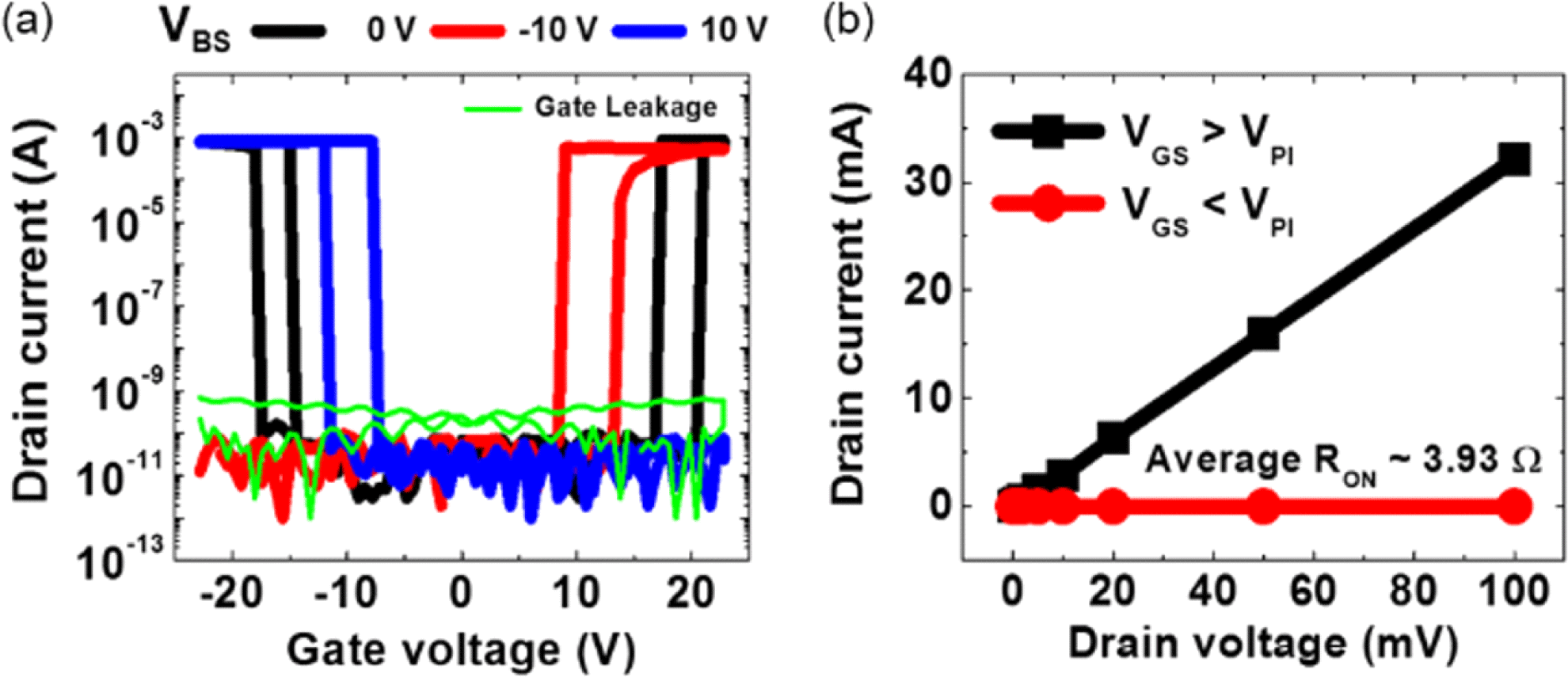
Fig. 3(a) shows the measured electrical switching characteristics and adjusted VPI and release voltage (VRL) of the printed 4T MEM relay by applying body-source voltage (VBS) of -10 V and 10 V. The abrupt switching characteristics exhibiting extremely low SS value below 1 mV and gate leakage was obtained with a VPI of 20.4 V and a hysteresis window of only ~3 V. This hysteretic switching window is attributed to the pull-in mode operation and surface adhesion forces between the movable beam and underlying drain electrode. The body bias of -10 V successfully adjusted the VPI of 20.4 V to 13.2 V, maintaining abrupt switching. This operation allows the realization of the complementary relay inverter by implementing p- and n-relays [16]. Because the RON consists of two metallic components (a metal-metal contact resistance between the beam and drain, and a resistance of the channel beam), extremely low a RON value of ~3.9 Ω was extracted from the VDS-IDS characteristics in Fig. 3(b). We will discuss various modes that lead permanent failure of inkjet-printed MEM relays.
To investigate the structural tolerance of the inkjet-printed MEM relays, the maximum cycling endurance was evaluated without biasing the VDS to eliminate the thermal effects, including welding or electromigration-related failures. After performing each cycling test by biasing 25 V-pulse with 0.5 Hz on the gate electrode, the current-voltage characteristics were measured by sweeping the VGS from 0 V to 25 V with a low VDS of 100 μV as shown in Fig. 4(a) due to the aforementioned reason. After 200 k cycling, the VPI was shifted in the negative direction while the VRL was maintained as shown in Fig. 4(b), which can be attributed to the reduced mechanical stiffness of the movable part. Because there are many vacancies, grain boundaries or structurally weak regions in the inkjet-printed printed beam formed using a nanoparticle-based Ag ink (diameter of Ag nanoparticles ~70 nm), cracks and creep can occur where structural stress is concentrated. During prolonged on/off switching cycles, the effective spring constant would be reduced, and the beam could eventually be broken and lose its restoring force, sequentially.
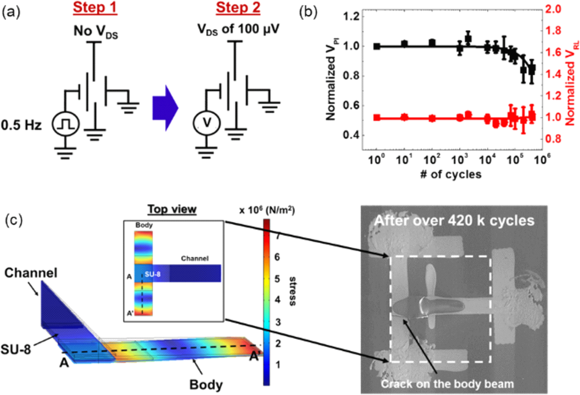
Fig. 4(c) shows the predicted structural stress distribution during the pull-in mode using 3-dimensional (3D) numerical finite-difference method (FDM) COMSOL Multiphysics with an AC/DC module. The deflection of the movable part was coupled with the electrostatic force between the gate electrode and the body beam generated by the electric field. By comparing the channel beam deflection as a function of the applied electrical potential and the contact gap between the channel beam and drain electrode, the VPI was determined to be 23.5 V. From the simulation results, the structural stress was concentrated near the junction area between the body beam and the orthogonally patterned SU-8 bonding layer. Since the distributed mechanical strain on the beam during the operation is proportional to the maximum deflection, most of the cracks were observed near the junction area on the center of the body beam where the maximum deflection occurred, as shown in the SEM image in Fig. 4(c).
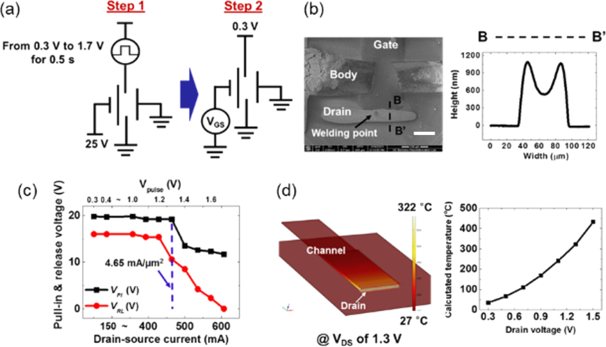
For inkjet-printed MEM relays using nanoparticle-type metallic inks, welding-induced failures by Joule heating at the contacting surfaces can be regarded as a dominant failure cause due to the high on-state current resulting from the extremely low contact resistance (<10 Ω) [13,14]. As the temperature of the contacting metal asperities increases during the operation, metal atoms at the contact could diffuse, leading to metal-to-metal bonds between the channel beam and drain electrodes. If the bonding energy is larger than the restoring force (=spring force), the MEM relays would be failed in a shorted state permanently. Especially, since the current flows through a high ridge in the edge of the drain electrode formed by the coffee-ring effect, the welding-related failures would be aggravated by high current density at the small contact area [10]. The voltage-pulses with various amplitudes from 0.3 V to 1.8 V were applied to the drain for 0.5 s during the on-state to investigate the maximum current flow capacity. Then, the I-V characteristics were measured by sweeping the VGS from 0 V to 25 V with a VDS of 0.3 V (Fig. 5(a)). The VPI and VRL were well-maintained until the VDS pulse with an amplitude of 1.3 V was applied during the on-state. However, the operation voltages (VPI and VRL) were shifted negatively as the amplitude of the VDS pulse increased over 1.3 V, then the channel beam eventually adhered to the surface of the drain electrodes when the VDS of 1.7 V was biased. This behavior was attributed to the thermal stress at the contact region generated by high current density, resulting in the welding-related failures and increasing stiction force between the channel beam and drain electrode. The welded point was observable on the ridge in the drain electrodes of the failed MEM relays as shown in Fig. 5(b). Considering the VDS, contact resistance and contacting area, we concluded that the maximum current density was 4.65 mA/μm2 as shown in Fig. 5(c). To further investigate, a thermal simulation was performed using 3D COMSOL Multiphysics. The channel width, length, gap between channel and drain, and Young’s modulus of channel were 95 μm, 365 μm, 0.5 μm, 41.19 Gpa, respectively. The calculated temperature of 322°C generated by the VDS of 1.3 V in the convective air also supported the welding-related electrically short-failure between the channel and drain (Fig. 5(d)). Note that inkjet-printed Ag layers generally have relatively lower thermal stability, specially Perelaer et al. reported the sudden resistance increase around 350°C [23].
We also performed cycling tests with different VDS from 0 to 100 mV (Fig. 6). Due to the metal-to-metal bonding by thermal stress, depending on the VDS, the mean number of cycles to failure (MCTF) was well-fitted to the following equation, which indicates that high VDS is one of the most critical parameters to accelerate welding-related failures leading high temperature [24].
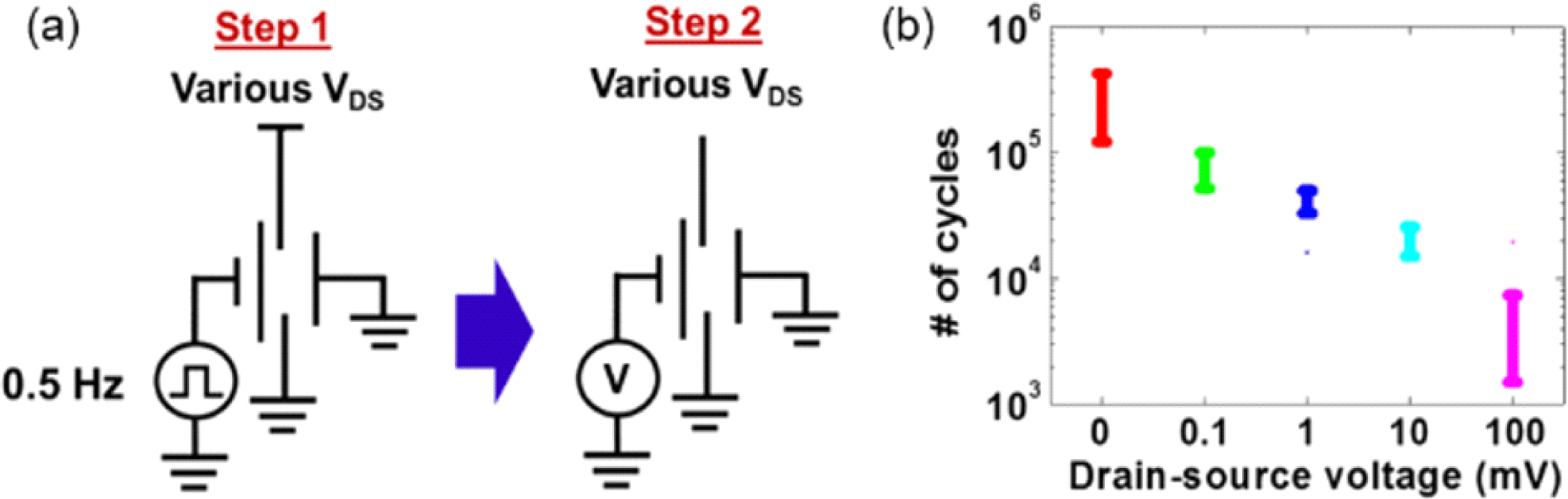
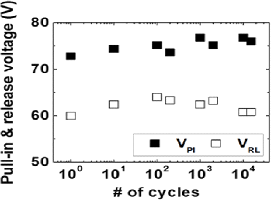
where A, EA, RON, KB, RC, and τ are a material-dependent pre-factor, the activation energy, the ON-state resistance, the Boltzmann constant, the contact resistance, and the thermal time constant respectively. From the experimental results, the endurance cycles were significantly reduced as increasing VDS due to joule heating-based heat generation. During the printed MEM relays operation, charges from the gate electrode can be injected over the energy barrier at the gate electrode and dielectric interface. If the injected charges are trapped in the gate dielectric when the MEM relays are in the on-state, it results in opposite effects to VPI and VRL enlarging the hysteresis window. The dielectric charging can lead to permanent device failures if the spring restoring force of the movable part cannot overcome the attractive coulomb force by the trapped charges. Because high gate bias can accelerate dielectric charging, a cycling test was performed with the printed 4T MEM relays exhibiting a high VPI of 72 V (Fig. 7). During the hot-switching cycles over 104, no significant shifts of the VPI and VRL were observed which indicates the dielectric charging is not a dominant issue to lead permanent device failures.
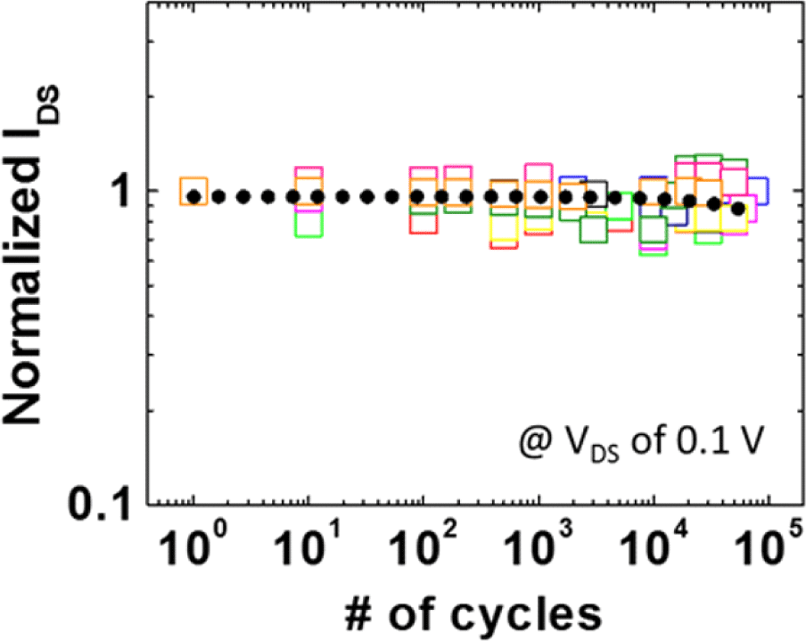
Since the MEM relays were operated under ambient conditions, the contacting area can be oxidized during hot-switching operation. The Ag electrodes are especially susceptible to oxide formation resulting in reduced IDS. Fig. 8 shows the results of degradation of the IDSduring the cycling tests. From the results of stable IDS during the hot-switching over 105, we could conclude that surface oxidation is not a critical issue for the switching operation. This behavior is also consistent with the previous result of 3-terminal printed MEM relays [10,13,14]. Note that the gate leakage-related failure occurred during the switching operation when the floated body beam touched the PVP gate dielectric layer due to an excessive electrostatic force.
4. CONCLUSION
In this paper, we analyzed the electrical and mechanical reliability of inkjet-printed 4T MEM relays in various failure modes: structural fatigue, welding by Joule heating, dielectric charging, and surface oxidation. The results of the cycling tests indicate that welding-related failures by Joule heating at the contacting area are the most critical issue for the reliability of the inkjet-printed 4T MEM relays. Especially, the high current density at the relatively small contact area and extremely low contact resistance can aggravate the welding issues. The simulation results obtained using COMSOL multiphysics supported the predicted distribution of the mechanical strain and thermal stress on the movable parts of the MEM relay. Based on our results, thermally and mechanically stable printable materials should be used for the realization of more reliable inkjet-printed MEM relays, for example, by introducing anti-friction coating to minimize the contact area and time or or using highly endurable conducting materials for the channel and drain against welding-related failures.