Journal of Flexible and Printed Electronics
Korea Flexible & Printed Electronics Society
RESEARCH

전기화학적으로 산화된 투과성 베이스 전극을 갖는 수직구조 유기 트랜지스터

이인혜1, 김연도1,2, 임경근1,2,*
In-Hye Lee1, Yun-Do Kim1,2, Kyung-Geun Lim1,2,*
1한국표준과학연구원(KRISS) 첨단오페란도분석팀
2과학기술연합대학원대학교(UST) 응용측정과학과
1Korea Research Institution for Standard Science (KRISS), Daejeon, Korea
2University of Science and Technology (UST), Daejeon, Korea
*Correspondence: kglim@kriss.re.kr

Author Contributions

IHL, KGL were involved in experiments, analysis, discussion, and drafting manuscript. YDK was involved in C-V measurement. All authors read and approved the final manuscript.

ⓒ Copyright 2022 Korea Flexible & Printed Electronics Society. This is an Open-Access article distributed under the terms of the Creative Commons Attribution Non-Commercial License (http://creativecommons.org/licenses/by-nc/4.0/) which permits unrestricted non-commercial use, distribution, and reproduction in any medium, provided the original work is properly cited.

Received: Oct 11, 2022; Revised: Nov 28, 2022; Accepted: Dec 13, 2022

Published Online: Dec 31, 2022

Graphical Abstract

jfpe-1-2-247-a1

ABSTRACT

Vertical organic thin film transistors (VOTFTs) are emerging electronic devices that can overcome the limitations of conventional organic thin film transistors (OTFTs) based on lateral architecture. Here, organic permeable base transistors (OPBTs) are formed with an oxide layer on the base electrode through an electrochemical process called anodization, and this oxide layer acts as a dielectric layer. Through this electrochemical method, the manufacturing process is simplified and the charge carrier transport of the VOTFT is improved. In this study, the thickness of AlOx formed by anodizing the Al electrode was calculated through the capacitance-voltage measurement of the metal-insulator-metal device, and OPBT operations were observed according to the anodizing potential and interfacial layer, respectively. In addition, we observed the specific behaviors of vertical OPBT depending on the applied potential correlations between middle base electrode and bottom collector electrode.

Keywords: Anodization; Aluminum oxide; Vertical organic thin film transistors (VOTFTs); Vertical organic transistors (VOTs); Organic permeable base transistors (OPBTs)

1. 서론

최근 유기 소재를 이용한 트랜지스터가 많은 연구 중에 있으며, 그 중에서도 수직 구조를 갖는 vertical organic transistor(VOT)는 채널(channel)이 수직(vertical) 방향으로 되어 있기 때문에 기존의 수평(lateral) 구조의 트랜지스터보다 on-current가 높으며, 반응 속도가 빠른 장점이 있다[1]. 수직 방향의 채널은 수평 구조의 채널에 비해 상대적으로 짧은 채널 길이를 갖는다. 이로 인해 수직 구조는 전자의 이동 거리가 짧아지면서 구동전압과 속도가 빨라진다. 또한, 베이스 전극에는 핀홀이 존재하여 전하 캐리어를 투과할 수 있게 하고 이것으로 인해 높은 전류 밀도 도달을 가능하게 한다[2]. 온 상태에서의 직렬저항감소 효과로 인하여 높은 전류밀도 값에 도달이 가능하다[3].

현재까지 다양한 구조의 수직구조 유기 트랜지스터가 연구되었는데[4], 그 중에서도 vertical organic permeable base transistor(VOPBT)는 베이스(base) 전극에 전계가 인가되었을 때 핀홀을 통해 수직방향으로 전자를 투과시키는 소자를 말하며[1], 그 결과 VOPBT는 보고된 유기 반도체를 이용한 트랜지스터 소자 중에서 가장 높은 수치인 40 MHz 수준의 transition frequency를 달성한 연구 결과가 보고되었다[5,6]. 알루미늄은 얇게 열 증착하면 핀홀이 자연적으로 발생하므로 유기 반도체 박막의 중간 위치에 스위칭 역할을 하는 투과 베이스 전극으로 활용된다[7]. 투과 베이스 전극은 소자가 온 상태(on-state)일 때 전자가 나노미터(nm) 크기의 핀홀을 통과하도록 하고 오프 상태(off-state)에서는 전자를 차단한다. 그러므로 핀홀은 전극을 가로질러 charge carrier transfer를 조절하는 효과가 있다. 하지만 기존의 산화 방법인 공기 노출 산화법은 산화층 형성이 불균일하며 미세 나노 구조를 제어할 수 없다는 평가를 받아왔다. 그에 비해, 전기화학적 산화법인 아노다이징은 Al 전극의 상하부 표면 뿐만 아니라, 수 나노미터(nm) - 수십 나노미터(nm) 크기의 핀홀 내부에 형성되어 베이스 누설 전류를 감소시키는 효과가 있다[1,8].

본 연구에서는 수직구조 유기 트랜지스터의 아노다이징을 이용하여 균일한 두께의 AlOx를 형성하여, 스위칭 속도의 상승과 누설 전류의 감소를 관찰하였다.

2. 연구방법과 소재 및 측정

소자 제작에 사용된 유리 기판은 기판을 세제, 아세톤, 이소프로필 알콜(IPA) 용액에서 각 10분씩 초음파 세척 후 건조하여 준비한다. 이후 바로 N₂ glove box로 이동 후 진공증착챔버(<10−7 mbar)로 이동하여 유기 반도체 층, 금속 전극 층, 픽셀 구분층(pixel define) 등을 증착했다.

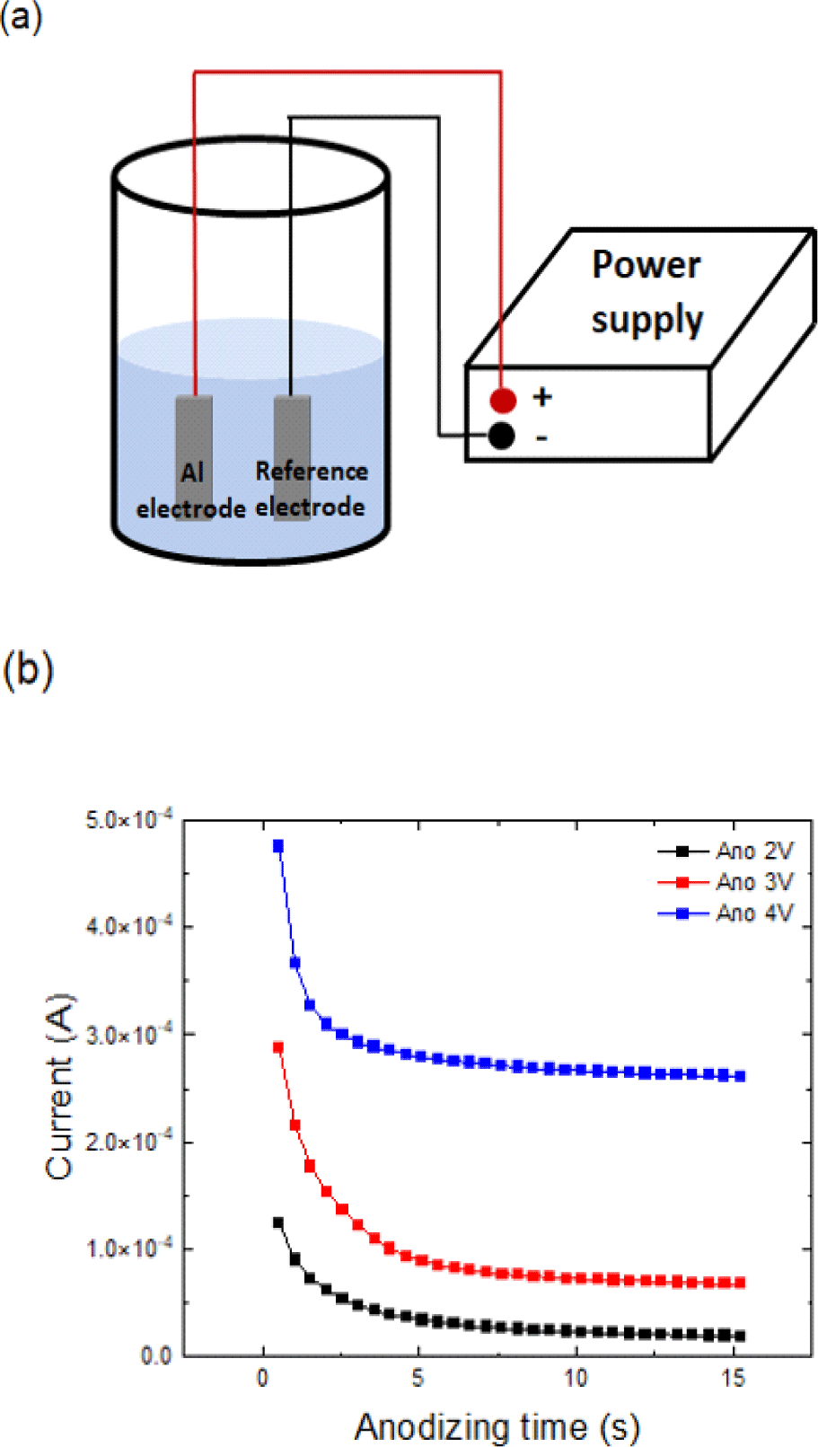
모든 박막의 형성은 열증착으로 진행하였으며 하부 소자의 조건은 다음과 같다. Ti 3 nm(0.5 Å/s);Au 50 nm(0.5 Å/s);Bottom C60 50 nm(0.5 Å/s);Al 25 nm(1 Å/s). 이후 glove box 내에서 150℃에서 30 min 동안 pre- heating을 진행한 후 공기로 꺼내 전기화학적 산화법인 아노다이징 과정을 진행하였다. 아노다이징을 위한 전해질은 0.01 M 구연산(2-hydroxypropane-1,2,3-tricarboxylic acid)을 탈이온수에 용해시켜 제조하였으며, Al 투과 베이스 전극까지 증착된 시료와 기준 전극을 전해질이 채워진 수조에 담근 후 움직이지 않게 조절하여 준다(Fig. 2(a)). 이후 DC 전원공급장치를 통해 아노다이징 bias potential를 가해주게 되면 알루미늄이 산화되어 표면에 산화 알루미늄 피막을 형성하게 된다. 아노다이징 진행 후 150℃에서 30 min 동안 post-heating 하여 수분을 날려준다. 이후 상부 소자 제작을 위한 소재의 증착 조건은 다음과 같다. Top C60 100 nm(0.5 Å/s); SiO 100 nm (0.5 Å/s); Al 100 nm(1 Å/s).

VOPBT의 전기적 측정은 글로브박스에서 Keithley 2636B SMU를 사용하여 진행하였으며, Capacitance-Voltage 측정은 Keithley 4200SCS parameter analyzer (Keithley Instruments, Cleveland, OH, USA)를 사용하였다.

3. 결과 및 고찰

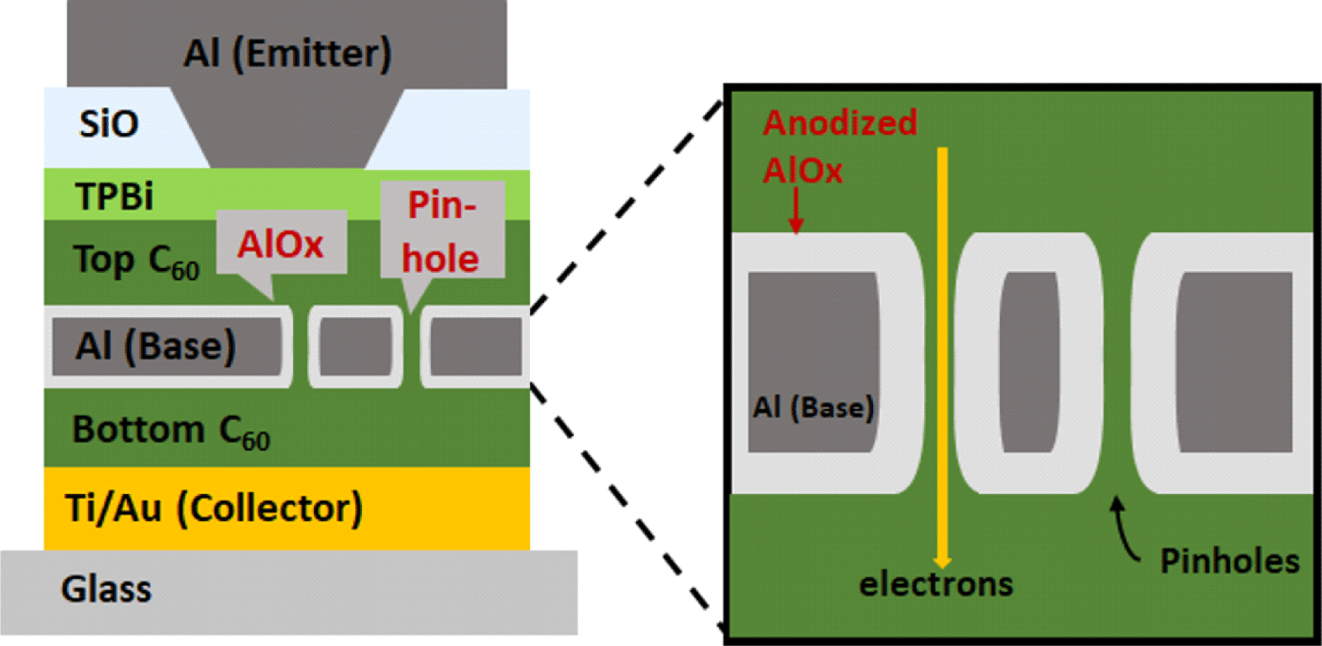
Fig. 1은 VOPBT의 구조와 아노다이징 된 base 전극을 보여준다. Ti/Au는 collector 전극으로 사용하였으며 하부(bottom), 상부(top) 유기 반도체로 C60를 증착하였다. Base 전극으로 사용하기 위해 Al 전극을 증착하였고, Pixel define을 위해서 SiO를 증착하였으며, 에미터(emitter) 전극으로 Al 전극을 가장 상부에 증착한 구조를 갖는다. 투과전극으로 사용된 알루미늄층을 base 전극으로 사용하기 위한 산화막 공정이 필요하기 때문에 전기화학적 산화법인 아노다이징 과정을 통해 나노미터(nm) 단위의 균일한 산화막을 생성하였다.

jfpe-1-2-247-g1
Fig. 1. Device schematic architectures of vertical organic permeable base transistors (VOPBTs) with anodized permeable electrodes.
Download Original Figure

아노다이징은 Al 전극에 얇은 산화막을 형성시켜 주는 방법이며 전해질로 Citric acid monohydrate를 사용하였다(Fig. 2(a)). 전체 소자구조에서 하부에 해당하는 Au(collector), C60(organic semiconductor), Al(base)까지 증착된 하부 소자를 전해질에 액침한 후 Al 전극에 potential을 가하면 Fig. 2(b)와 같이 전류가 감소 후 포화(saturation)된다. 즉, 전기화학적 반응에 의해서 Al이 AlOx로 산화되면서 reference 전극과 Al 전극 사이의 전류가 감소하게 되고, 특정 반응시간(15∼180 s)이 지난 후 AlOx 막의 두께가 두꺼워지면서 Al의 아노다이징 반응이 감소하게 되어 전류가 포화되었다. 또한 아노다이징 potential을 2, 3, 4 V로 증가시킬수록 전류 레벨(current level)이 감소하는 것을 확인하였으며, 이것은 AlOx 두께의 증가에 의한 영향을 받는다.

jfpe-1-2-247-g2
Fig. 2. VOPBTs with anodization middle electrode (base electrode). (a) Schematic of the anodizing method. (b) Current level measurement by anodizing voltage.
Download Original Figure

아노다이징 조건에 따른 AlOx의 두께 변화를 관찰하기 위해 Metal-Insulator-Metal(MIM) device를 제작하여 Capacitance-Voltage 측정을 진행하였다(Fig. 3).

jfpe-1-2-247-g3
Fig. 3. Capacitance density measurement of metal-insulator-metal (MIM) device. Inset figure shows the MIM with Al-anodized AlOx-Au.
Download Original Figure

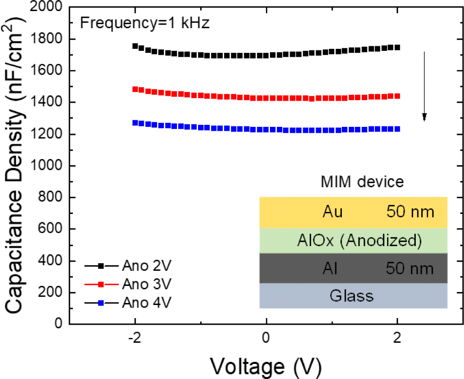
소자의 구조는 Al 50 nm(1 Å/s); anodized AlOx; Au 50 nm(0.5 Å/s)이며, 1 kHz의 일정한 주파수(frequency) 에서 커패시턴스 밀도(capacitance density)를 측정하였다. 아노다이징 potential을 증가시킬수록 Al 층 상단의AlOx가 두꺼워져 capacitance density가 감소하였다. 또한 capacitance density값을 이용하여 실제 형성된 AlOx의 두께를 계산하였다. Table 1에 아노다이징 potential에 따른 MIM 소자의 capacitance density 및 두께를 평균하여 나타냈다. AlOx 두께의 계산에 사용한 커패시턴스(capacitance) 계산 공식은 다음과 같다.

Table 1. Capacitance density and AlOx thickness as the anodizing voltage increases
Anodizing voltage (V) Capacitance density (nF/cm2) AIOx thinkness (nm)
2 V 1,711.6 4.7
3 V 1,436.6 5.5
4 V 1,234.5 6.5
Download Excel Table
C = 0 A d
(1)

C=Capacitance

A=Pixel area

d=Thickness

ε=Dielectric constant

ε0=8.854×10⁻¹² F/m

2 V로 아노다이징 된 소자에서, AlOx의 두께는 4.7 nm로 계산되었고 아노다이징 potential을 3, 4 V로 증가할수록 AlOx의 두께도 각각 5.6 nm, 6.5 nm로 증가하는 경향을 보였다(Table 1). 이를 통해 아노다이징 potential을 증가시킬수록 capacitance density값은 낮아지며, 이것은 아노다이징된 AlOx 피막의 두께 증가를 의미한다.

Base 전극에 아노다이징을 진행한 VOPBT의 transfer 특성을 측정하였다(Fig. 4). 도면에서 실선은 collector 전류, 점선은 base 누설 전류를 의미한다. 또한 transfer 특성에서 operating parameter들을 분석하여 Table 2에 표기하였다. Collector-emitter voltage를 1 V로 고정하고 base-emitter voltage를 −1 V to 1 V 조건으로 sweep하였을 때, Fig. 4와 같이 아노다이징 potential이 2, 3, 4 V로 증가함에 따라 base 전류(누설 전류)가 전체적으로 감소하는 경향을 보였다. 이것은 Fig. 3Table 1에서 보았듯이, 높은 아노다이징 potential로 산화를 진행할수록 AlOx의 두께가 두꺼워져 누설전류가 하락하는 것으로 보인다. 또한 on-current가 감소하지만 off-current가 더욱 크게 감소하였기 때문에 on/off ratio의 증가를 확인할 수 있다. VTH (threshold voltage)의 증가도 확인할 수 있는데, 이것은 base 전극에서 일어나는 charge trapping에 기인한다고 볼 수 있다[9]. VOPBT의 주요한 매개 변수(parameter)인 투과율(permeability)은 emitter 전류(IE)에 대한 collector 전류(IC)의 비율이며, 다음 수식으로 나타낼 수 있다[1].

jfpe-1-2-247-g4
Fig. 4. Electrical properties of VOPBTs. Transfer curves of VOPBTs with anodizing potential 2, 3, and 4 V.
Download Original Figure
Table 2. Operating parameters of VOPBTs with various anodizing potential
Ano 2 V Ano 3 V Ano 4 V
On current 4.2×10⁻⁷ 2.6×10⁻⁷ 1.5×10⁻⁷
Off current 6.5×10⁻⁹ 1.1×10⁻⁹ 3.9×10⁻¹⁰
Gate leakage current 2.1×10⁻⁹ 1.7×10⁻¹⁰ 1.3×10⁻¹⁰
VTH −0.03 0.16 0.36
On/off ratio 1.6×10² 4.1×10³ 2.5×10³
Permeability 99.50% 99.93% 99.91%
Download Excel Table
P e r m e a b i l i t y = I c I E = I C I B + I C
(2)

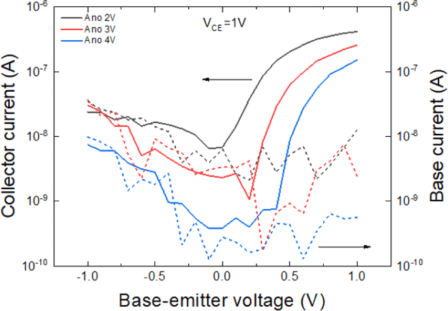
아노다이징 potential이 1 V에서 3 V로 증가하였을 때 VOPBT 소자에서 투과율(permeability)이 99.50%에서 99.93%로 증가하였다. 즉, charge carrier가 핀홀을 통해 base 전극을 가로질러 이동하기 때문에, 핀홀을 포함한 base 전극 표면에 아노다이징을 통하여 AlOx 형성을 제어하여, Base 전극으로의 누설 전류(IB)를 억제하고 투과율(permeability)의 증가를 관찰하였다.

Fig. 5에서는 상부 계면 물질(top interface material)을 추가하여 제작한 VOPBT의 transfer 특성을 보여준다. 반도체 소자에서 금속 전극과 반도체 물질 사이의 계면은 중요한 역할을 하는데, 이것은 접촉 금속(contact metal)과 유기 반도체 사이에 정공 또는 전자가 풍부한 계면층(interface layer)을 포함하면 접촉(contact) 영역을 국부적으로 도핑할 수 있는 효과가 있기 때문이다[10]. 기존 수평구조의 유기 트랜지스터에서 상부 계면층(top interlayer)은 전자의 주입(injection)을 증가시키는 효과가 있는 것으로 알려져 있다[11,12]. VOPBT의 계면층(interlayer) 소재는 TPBi (1,3,5-Tris(1-phenyl-1H-benzoimidazol-2-yl)benzene)를 사용하였으며, collector-emitter 전압은 3 V로 일정한 조건 하에서 측정을 진행하였다. Without interlayer와 TPBi를 사용한 소자는 10−8 A 수준의 비슷한 off-current를 보였으나 TPBi를 사용한 소자는 without interlayer 조건보다 on-current가 약 2배 상승하였다. 이것은 앞서 설명한 바와 같이 전자의 injection 을 증가시키는 효과가 있기 때문으로 예상된다. 또한 without interlayer 조건의 소자보다 TPBi interlayer 를 사용한 조건에서 base 전류(누설 전류)가 10−8∼10−9 A 정도로 낮게 측정된 것을 확인하였다.

jfpe-1-2-247-g5
Fig. 5. Electrical properties of VOPBTs. Transfer curves of VOPBTs with or without interlayer (TPBi) between top organic semiconductors and emitter electrode.
Download Original Figure

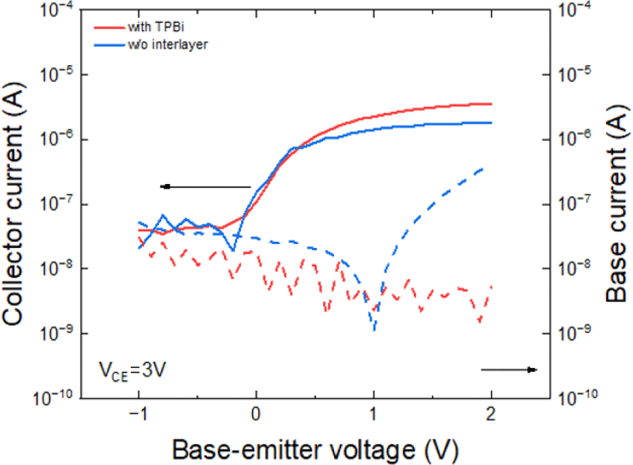
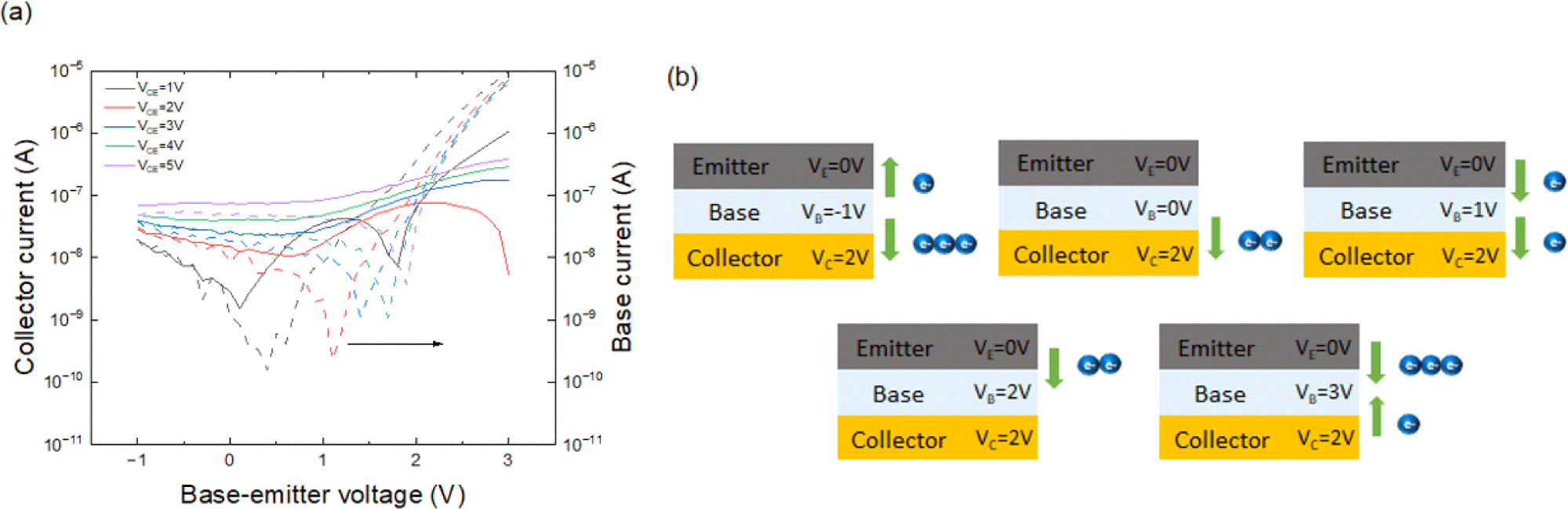
Fig. 6(a)는 collector-emitter 사이의 전압(VCE)을 각 1 V에서 5 V 범위에서 1 V씩 증가시키며 transfer 특성을 관찰하였다. Collector 전류의 절반 값에 해당하는 부분의 collector-emitter voltage에서(VE=0 V, VBE= 1 V, VCE=2 V), base 전극에 들어오거나 나가는 전류가 동등하기 때문에 base 누설전류가 가장 낮은 값을 갖는다(Fig. 6(b)). 또한 VCE가 클수록 base 전류가 가장 낮은 VBE 값(VBE,Min)이 right shift 되는 현상을 보인다. 또한 VBE,Min는 VCE의 절반에 준하는 값을 유지하는 것으로 관찰되었다. 이것은 소자 구조의 영향이 큰데, 수직 구조 트랜지스터는 collector와 emitter가 투과 베이스 전극(permeable base electrode)을 중간에 두고 유기 반도체를 가로질러 수직으로 맞닿아 있는 구조이기 때문에 나타나는 현상으로 볼 수 있다.

jfpe-1-2-247-g6
Fig. 6. Electrical properties of VOPBTs depending on measurement. (a) Transfer curves of VOPBTs with various VCE (b) The relative potentials and the resulting electron transports in VOPBTs.
Download Original Figure

4. 결론

수직구조 유기 트랜지스터의 투과 전극에 간단한 전기화학적 방법인 아노다이징을 이용하여 산화막의 미세 형상을 제어하고 계면층을 삽입하여 VOPBT의 성능이 크게 증가하는 것을 보고하였다.

아노다이징 공정을 통해 투과전극의 상하부뿐 아니라 핀홀 내부까지 아노다이징 potential에 비례하여 결정되는 균일한 두께의 AlOx 절연막을 형성하였다. 아노다이징 potential이 2, 3, 4 V로 증가하면 off-current가 10−9 A에서 10−10 A으로 감소하였으며, base 누설전류도 10−10까지 감소하였다. 그 결과 아노다이징 potential 4 V에서 on/off ratio는 2 V보다 높은 값인 103로 측정되었다.

또한 emitter 전극에 without interlayer와 with interface material(TPBi)에 따른 VOPBT 구동을 비교하여 TPBi interlayer을 사용한 소자는 base 전류가 최대 100배 이상 낮게 측정되었으며, on-current 또한 약 2배 상승하였다.

기호설명

VOT:

Vertical organic transistor

OPBT:

Organic permeable base transistor

VOPBT:

Vertical organic permeable base electrode transistor

MIM:

Metal-insulator-metal

Funding

This work was supported by the National Research Foundation of Korea (NRF) grant funded by the Korea government (MSIT) (NRF-2022M3H4A1A03076280).

Declarations of Competing Interests

The authors declare that they have no competing interests.

REFERENCES

[1].

Dollinger, F.; Lim, K.; Li, Y.; Guo, E.; Formánek, P.; Hübner, R.; Fischer, A.; Kleemann, H.; Leo, K. Vertical Organic Thin-Film Transistors with an Anodized Permeable Base for Very Low Leakage Current. Adv. Mater. 2019, 31 (19), 1900917.

[2].

Klinger, M. P.; Fischer, A.; Kaschura, F.; Widmer, J.; Kheradmand-Boroujeni, B.; Ellinger, F.; Leo, K. Organic Power Electronics: Transistor Operation in the KA/Cm2 Regime. Sci. Rep. 2017, 7 (1), 44713.

[3].

Klinger, M. P.; Fischer, A.; Kaschura, F.; Scholz, R.; Lüssem, B.; Kheradmand-Boroujeni, B.; Ellinger, F.; Kasemann, D.; Leo, K. Advanced Organic Permeable-base Transistor with Superior Performance. Adv. Mater. 2015, 27 (47), 7734-7739.

[4].

Kleemann, H.; Krechan, K.; Fischer, A.; Leo, K. A Review of Vertical Organic Transistors. Adv. Funct. Mater. 2020, 30 (20), 1907113.

[5].

Kheradmand-Boroujeni, B.; Klinger, M. P.; Fischer, A.; Kleemann, H.; Leo, K.; Ellinger, F. A Pulse-Biasing Small-Signal Measurement Technique Enabling 40 MHz Operation of Vertical Organic Transistors. Sci. Rep. 2018, 8 (1), 7643.

[6].

Klinger, M. P.; Fischer, A.; Kleemann, H.; Leo, K. Non-Linear Self-Heating in Organic Transistors Reaching High Power Densities. Sci. Rep. 2018, 8 (1), 9806.

[7].

Zhao, K.; Deng, J.; Wu, X.; Cheng, X.; Wei, J.; Yin, S. Fabrication and Characteristics of Permeable-Base Organic Transistors Based on Co-Evaporated Pentacene: Al Base. Org. Electron. 2011, 12 (6), 1003-1009.

[8].

Guo, E.; Wu, Z.; Darbandy, G.; Xing, S.; Wang, S. J.; Tahn, A.; Göbel, M.; Kloes, A.; Leo, K.; Kleemann, H. Vertical Organic Permeable Dual-Base Transistors for Logic Circuits. Nat. Commun. 2020, 11 (1), 4725.

[9].

Powell, M. Charge Trapping Instabilities in Amorphous Silicon-silicon Nitride Thin-film Transistors. Appl. Phys. Lett. 1983, 43 (6), 597-599.

[10].

Liu, C.; Xu, Y.; Noh, Y. Y. Contact Engineering in Organic Field-Effect Transistors. Mater. Today 2015, 18 (2), 79-96.

[11].

Bachelet, A.; Chabot, M.; Ablat, A.; Takimiya, K.; Hirsch, L.; Abbas, M. Low Voltage Operating Organic Light Emitting Transistors with Efficient Charge Blocking Layer. Org. Electron. 2021, 88, 106024.

[12].

Li, S. H.; Xu, Z.; Ma, L.; Chu, C. W.; Yang, Y. Achieving Ambipolar Vertical Organic Transistors via Nanoscale Interface Modification. Appl. Phys. Lett. 2007, 91 (8), 083507.