
1. INTRODUCTION
Metasurfaces, composed of periodic nanostructures, have been attractive because of their fine control of electromagnetic waves, which is used in various applications such as holograms, lenses, and other optical systems [1-3]. In order to create metasurfaces with a resolution below 10 nm, the commonly employed technique is electron-beam lithography (EBL). This method involves the direct exposure of an electron-sensitive resist to a high-voltage electron beam, which shapes the resist to the desired form [4-5]. EBL offers the advantage of maskless fabrication, providing significant design freedom. Additionally, the short wavelength of electrons enables the realization of high-resolution structures [4,6]. However, EBL requires expensive high-vacuum systems equipped with magnetic lenses to precisely control the electrons. Consequently, it suffers from low throughput, limiting the mass production of nanostructures. To address this limitation and achieve mass production of metasurfaces, several optical nanofabrication techniques have been explored, including holographic lithography [7-13] and plasmonic lithography [14-20]. Nevertheless, these methods encounter the same inherent drawbacks of optical nanopatterning, such as the diffraction limit.
To overcome these limitations, mechanical nanofabrication has been researched, of which representative is nanoimprint lithography (NIL). In contrast to optical nanopatterning methods, NIL relies on straightforward mechanical procedures to fabricate nanostructures, resulting in various NIL-based techniques [21-23]. Typically, a rigid mold with nanopatterns is pressed into a resin composed of polymeric material with consistent energy to transfer the nanopatterns on-to the resin. Unfortunately, the NIL resin has a general refractive index of about 1.6, which is too low to manipulate electromagnetic waves. To increase the refractive index of the resin, the imprinted nanostructures with the low-refractive-index resin were coated with a high-refractive-index material, which resulted in an effective refractive index higher [24]. Titanium dioxide (TiO2) thin film with a high refractive index of about 2.5 was deposited by using an atomic layer deposition (ALD) system onto the metasurfaces fabricated by the ultraviolet (UV) NIL process. This efficiently modulated visible light in a confined tiny volume, achieving high conversion efficiency of over 77% at 532 nm.
Moreover, TiO2 nanoparticle-embedded resin (nano-PER) was directly imprinted with a single step to fabricate metasurfaces [25]. By mixing the high-refractive-index material with the low-refractive-index resin, the effective refractive index of the TiO2 nano-PER was increased by 1.9. With sophisticated structure optimization of the effective resin, the metasurface was simply printed and it also realized high conversion efficiency of 90% at 532 nm. In addition, the modulation of the surface energy of various interfaces during the process led to the easier transfer of metasurfaces from the soft mold. Besides TiO2, various nanoparticles such as silicon and zirconium dioxide were adopted for the highly efficient metasurface at broad wavelengths [26-27]. This one-step nanofabrication technique for metasurfaces can open new avenues because of its unprecedented high productivity. Nevertheless, there are still technical issues for the uniform fabrication of metasurfaces.
In this study, we investigate processing factors in detail for the effective nano-PER NIL process. After a concise introduction of the mechanism of the nano-PER NIL process, the advantages of the nano-PER NIL process are shown with the fabrication of simple nanopillars and nanoholes. Next, mechanical analysis is conducted for high-aspect-ratio nanostructures with sub-100 nm widths, which is applied to fabricate high-resolution metasurface. The soft mold composed of Polydimethylsiloxane (PDMS) is swelled by solvents included in the nano-PER. The isotropic expansion of PDMS distorts metaatom structures. Likewise, the UV curing time of the nano-PER is discussed for the uniform fabrication of metasurfaces. Through optimized processing conditions, we fabricate metasurfaces with various dimensions to verify the successful optimization of the nano-PER NIL process. Finally, we fabricate the high-performance metasurface by the established nano-PER NIL process and realize the vivid metaholographic image.
2. METHODS
The fabrication method of the master mold was described in Fig. 1(a). A Si substrate was used for the master mold. The meta-atoms were transferred onto a bilayer of two positive tone photoresists (495 PMMA A6, MicroChem & 950 PMMA A2, MicroChem) using the standard EBL process (ELIONIX, ELS-7800; acceleration voltage: 80 kV, beam current: 100 pA). The exposed patterns were developed by MIBK/IPA 1:3 developer mixed solution. An 80 nm-thick chromium (Cr) layer was deposited using electron beam evaporation (KVT, KVE-ENS4004). The lifted-off Cr meta-atoms were used as an etching mask for the Si substrate. Cr patterns were transferred onto the Si substrate using a dry etching process (DMS, silicon/metal hybrid etcher). The remaining Cr etching mask was removed by Cr etchant (CR-7).
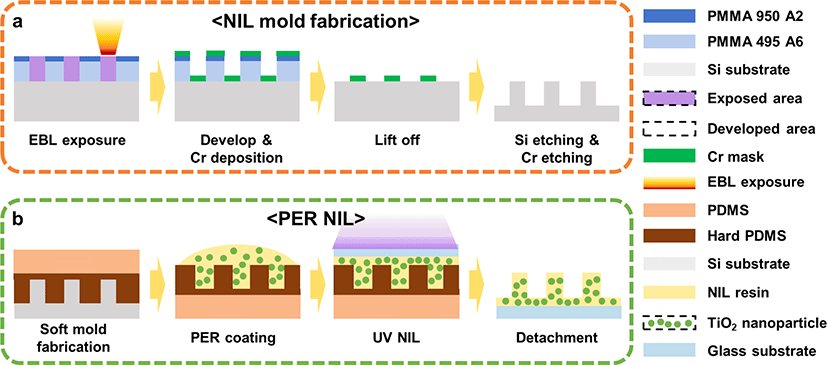
h-PDMS was prepared by mixing 3.4 g of vinylmethyl copolymers (VDT-731, Gelest), 18 μL of platinum-caralyst (SIP6831.2, Gelest), 0.1 g of the modulator (2,4,6,8-tetramethyl-2,4,6,8-tetravinylcyclotetrasiloxane, Sigma-Aldrich), 2 g of toluene, and 1 g of siloxane-based silane reducing agent (HMS-301, Gelest). The h-PDMS was spin-coated on the master mold at 1,000 rpm for 60 s, then baked at 70? for 2 h. A mixture of a 10:1 weight ratio of PDMS (Sylgard 184 A, Dow corning) and its curing agent (Sylgard 184 B, Dow corning) was poured on the h-PDMS layer and cured at 80? for 2 h. The cured soft mold was detached from the master mold, then used to replicate the nano-PER structure.
The TiO2 nano-PER was prepared by mixing TiO2 NPs dispersed in MIBK (DT-TIOA-30MIBK (N30), Ditto Technology), monomer (dipentaerythritol penta-/hexa-acrylate, Sigma-Aldrich), photo-initiator (1-Hydroxycyclohexyl phenyl ketone, Sigma-Aldrich), and MIBK solvent (MIBK, Duksan General Science). The mixing ratio was controlled to achieve a weight ratio of 4 wt % for TiO2 NPs, 0.7 wt% for monomer, and 0.3 wt % for the photo-initiator.
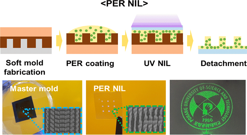
The fabrication method of the TiO2 nano-PER NIL process was discussed in Fig. 1(b). The mixed TiO2 nano-PER was drop coated on the fabricated soft mold. By absorbing solvents in TiO2 nano-PER, the soft mold was swelled, and the TiO2 nanoparticles were embedded in the soft mold well. With control of UV curing energy between 5∼10 J/cm2, the TiO2 nano-PER was cured at a constant pressure of 2 bars and detached subsequently.
The scanning electron microscopy (SEM) images were taken using a JEOL JSM-6700F field-emission SEM (typical operation voltage: 5 kV). A 532 nm laser (532 nm diode-pumped solid-state lasers, Thorlabs) was incident on a linear polarizer (Ø 1/2” unmounted linear polarizers, Thorlabs), half-wave plate (Ø 1/2” mounted achromatic half-wave plates, Thorlabs), and a quarter-wave plate (Ø 1/2” mounted achromatic quarter-wave plates, Thorlabs) to form right circular polarized (RCP) light. A 500 μm diameter pinhole (P500HD - Ø1/2” (12.7 mm) Mounted Pinhole, Thorlabs) was used to block the unnecessary light.
3. RESULTS AND DISCUSSION
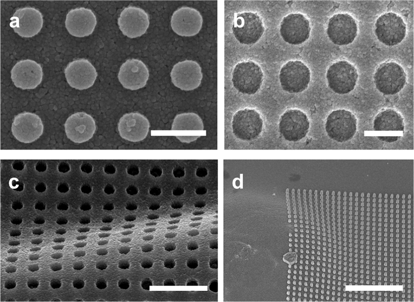
The TiO2 nano-PER NIL process realizes simple nanopattern arrays on any surface by using the mechanical printing technique. Nanopattern arrays with 280-nm width, 490-nm period, and 200-nm height have been fabricated entirely (Fig. 2(a)). In addition, the shape of the fabricated nanopillars is clear. Also, the nanohole arrays with 400-nm width, 630-nm period, and 200-nm depth, which correspond to a reversed shape of nanopillars, have been also realized (Fig. 2(b)). Through these results, the TiO2 nano-PER NIL process can secure successful transfer of any kind of simple nanostructure. Besides, nanoparticles mixed with the NIL resin have fluidity unlike conventional rigid thin film, so the fabricated nanostructures can be flexible and durable to any stimulus (Fig. 2(c)). In addition, the TiO2 nano-PER was covered overall and the nanopatterns were transferred on an impurity of the glass substrate (Fig. 2d), which can be printed on any arbitrary surface due to the mechanical printing technique of the TiO2 nano-PER NIL process.
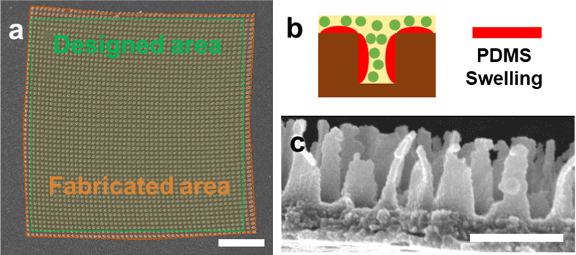
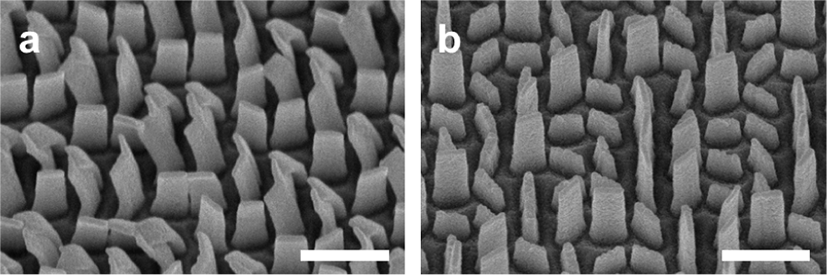
Despite the superior processability for any nanostructure, it is equivalent to low-aspect-ratio nanopatterns. To fabricate high-aspect-ratio metasurfaces, there are lots of obstacles in the TiO2 nano-PER NIL process. Among them, the swelling effect of the soft mold by absorption of solvents is the most important. During the swelling phenomenon, the soft mold contacting solvents in the TiO2 nano-PER locally expands and results in an unintended distortion of the transfer area, as shown in Fig. 3(a). Because of the distorted area, the modulation of light is also affected such as a hologram distortion and lower focusing efficiency of lenses. Metaatoms are also influenced by the swelling effect (Fig. 3(b)). When the TiO2 nano-PER permeate in the nanohole structures, the nearest surface of the soft mold is swelled by the solvent, disturbing a robust accumulation of particles in the nanohole. This causes broken or imperfect nanostructures as seen in Fig. 3(c). Therefore, for the intact realization of high-aspect-ratio metasurfaces, the metasurface design considering the swelling effect of the soft mold should be conducted. Because the swelled PDMS expands isotopically, a directional control of the swelling effect is challenging. Although, the PDMS swelling effect can be weakened by using solvents with a low swelling ratio [28], which is currently under development for our following reports.
UV curing energy during the TiO2 nano-PER NIL process is also a crucial factor to make delicate metasurfaces. When insufficient UV energy of about 5 J/cm2 is applied in the TiO2 nano-PER, the metaatoms with high aspect ratio are not fully cured and they are bent after the detachment of the soft mold because of their soft polymer chains, as shown in Fig. 4(a). On the other hand, excessive UV energy about 10 J/cm2 causes hard polymer chains in the fabricated metaatom, which are not flexible to an external force. Therefore, the high-aspect-ratio metaatoms are broken during the detachment step (Fig. 4(b)). As a result, the proper UV curing energy can secure both high flexibility and fabrication yield of metasurfaces.
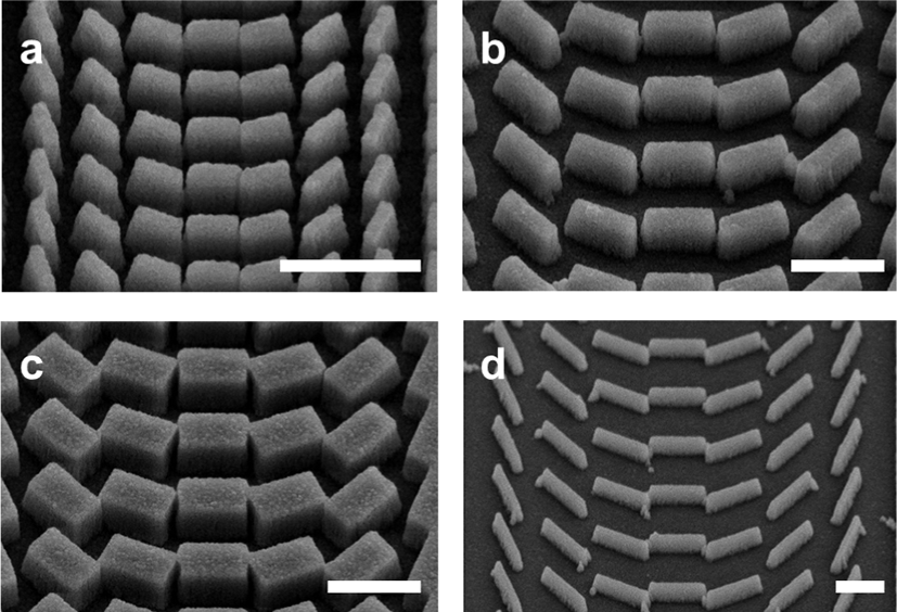
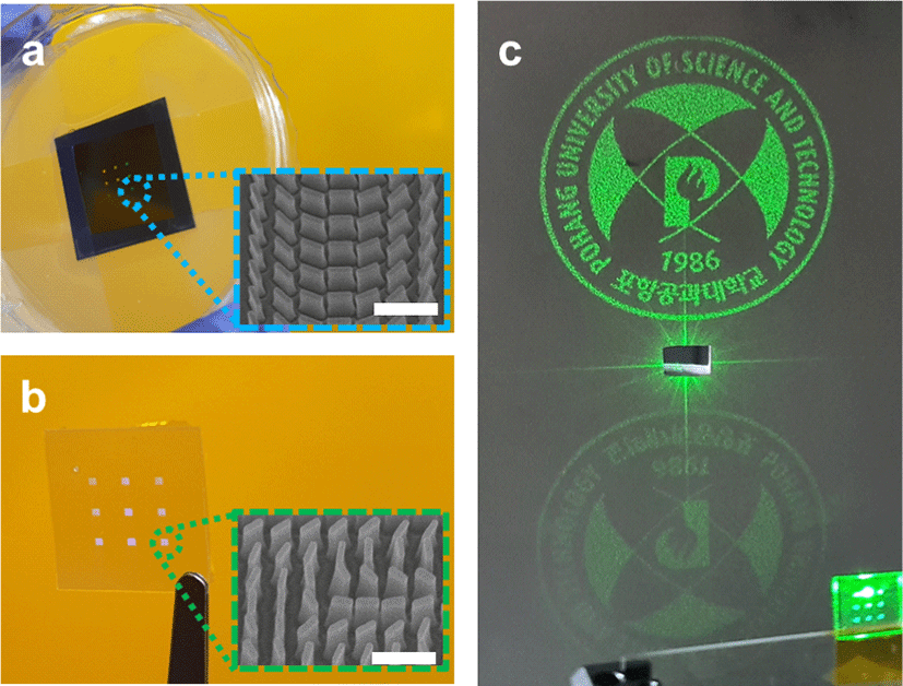
By using the optimized TiO2 nano-PER NIL process, metasurfaces with various dimensions can be successfully fabricated. Especially, high-aspect-ratio metasurfaces are also realized by the single-step NIL process, as shown in Fig. 5. Furthermore, the finally optimized master mold considering experimental corrections is fabricated (Fig. 6(a)) and thus the metasurface transferred by the TiO2 nano-PER NIL process is perfectly matched with the metasurface design (Fig. 6(b)). The simulated and measured conversion efficiency was 96.9% and 90.6% at 532 nm, respectively [25]. Thus, the fabricated metasurface shows the vivid hologram images at 532 nm (Fig. 6(c)), verifying that the metasurface is replicated well as planned.
4. CONCLUSION
In conclusion, we investigated the processing factors of the TiO2 nano-PER NIL process. While the low-aspect-ratio nanopatterns can be easily transferred by the TiO2 nano-PER NIL process, there are some considerations to fabricate precise high-aspect-ratio nanopatterns. First, the swelling effect can be considered to not distort the intended metaatoms. Second, UV curing energy can control the mechanical properties of the printed nanostructures. By paying attention to these parameters, we can fabricate high-aspect-ratio metasurfaces with a single step. Over two-dimensional metasurfaces, three-dimensional metasurfaces will be directly fabricated with fine tuning of metaatom shapes such as slanted nanostructures by using these nanofabrication techniques [29]. We expect that this simple but powerful nanofabrication will open up the commercialization of metasurfaces.