
1. INTRODUCTION
Polymer light-emitting diodes (PLEDs) have been regarded as a great promise for flexible display application due to their low cost and ease of fabrication [1]. However, their electron injection materials, such as calcium (Ca) and lithium fluoride (LiF), are sensitive to air and require encapsulation, rendering roll-to-roll (R2R) device fabrication challenging. To overcome this limitation, inverted structure PLEDs (IPLEDs) which use metal oxides as electron injection layers have emerged as a promising alternative [2-5]. These IPLEDs offer advantages such as solution processability and air stability, making them suitable for the R2R fabrication of flexible displays.
Despite the great progress in IPLEDs, most reported IPLEDs have been fabricated on indium tin oxide (ITO)/glass substrates, which are brittle and unsuitable for flexible displays. Researchers have attempted to address this issue by fabricating IPLEDs on flexible plastic polymer substrates (e.g., polyethylene terephthalate (PET)) with flexible electrodes (e.g., graphene, silver nanowire, gold grid) [6-8]. However, plastic substrates suffer from poor thermal stability and gas-oxygen permeability, limiting their broad applications in displays. Additionally, achieving uniform film deposition of flexible electrodes on these substrates is a complex process. Therefore, it is important to explore simplified materials that can serve as both a flexible metal and substrate.
Metal foils, such as stainless steel (STS), offer promising characteristics as flexible substrates and electrodes in flexible displays. They possess desirable properties including flexibility, excellent thermal stability, gas-oxygen non-permeability, high conductivity, good heat dissipation, and low cost. Notably, STS exhibits interfacial stability and significantly lower electrical resistance (<10−6 ohm/sq) compared to ITO (∼10 ohm/sq), making it suitable for use as both a substrate and an electrode. Although small-molecule organic light-emitting diodes with normal structure based on STS substrates have been reported [9], they typically utilize a brittle SiO2 insulating layer on the STS to smoothen the surface and prevent electrical short circuits in devices and deposit 300 nm of Ag on top of the SiO2 layer as an anode. To the best of our knowledge, there is no previous report on the use of STS as both an electrode and substrate in IPLEDs and organic light-emitting diodes.
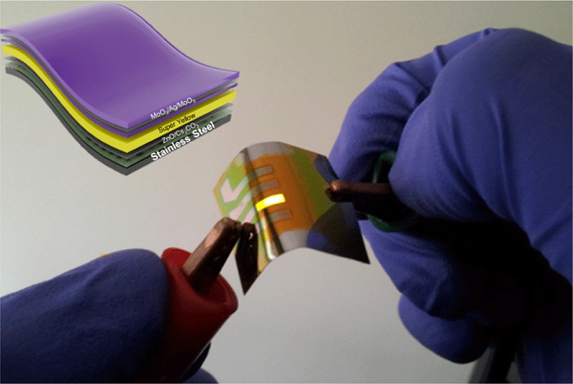
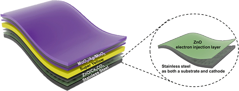
In this paper, we present the first air-stable IPLEDs on STS, wherein STS serves as both the cathode and substrate simultaneously (Fig. 1). We employ mechanical and chemical planarization steps to improve the surface roughness of STS, achieving a uniform surface morphology. A zinc oxide (ZnO) layer is subsequently deposited on top of STS to further reduce surface roughness and enhance electron injection into the polymer emitting layer. An electron injection interlayer, cesium carbonate (Cs2CO3), is then introduced on the ZnO layer to facilitate the electron injection barrier to the emitting layer. Finally, we optimize a MoO3/Ag/ MoO3 multilayer as a highly transparent, semi-transparent anode positioned on the polymer emitting layer, thereby demonstrating the flexible and air-stable IPLEDs on an STS cathode/substrate.
2. METHODS
A mechanically and chemically planarized stainless steel (STS) substrate (Taewon scientific Co. Ltd) was used for both a substrate and a cathode. A patterned 350 nm SiO2 layer was deposited on STS substrate by sputtering to confine the device pixel and prevent the short current in a device. The SiO2-patterned metal substrates were cleaned by sonication in acetone (twice) and isopropanol (once) for 15 minutes each. A 22-nm thick layer of zinc oxide (ZnO) was deposited on the cleaned STS substrate by sputtering. Then, the substrate was transferred to nitrogen-filled glove box and then cesium carbonate (Cs2CO3), dissolved in 2-ethoxyethanol at a concentration of 5 mg mL-1, was spin-coated onto the STS/ZnO substrate. Super Yellow (Merck OLED Materials. GmbH, catalog number PDY-132), dissolved in toluene at a concentration of 0.9 wt%, was then spin-coated on top of the Cs2CO3 layer. The resulting film was baked at 100°C for 10 minutes to remove residual solvent. The device was transferred to a high-vacuum chamber (<10−7 Torr). MoO3 (5 nm) (powder, 99.99%, Sigma-Aldrich), Ag (15 nm), and MoO3 (45 nm) were sequentially deposited to form a transparent top anode. The current-voltage characteristics and electroluminescence properties of the IPLEDs that used STS were measured using a Keithley 236 source measurement unit and a Minolta CS2000 spectroradiometer.
3. RESULTS AND DISCUSSION
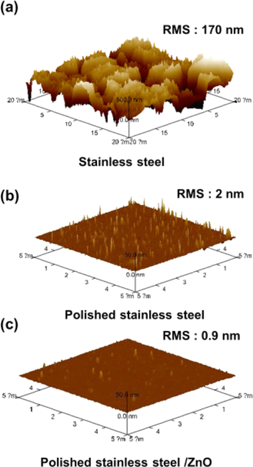
To enable the operation of IPLEDs using STS as both a cathode and substrate, it is essential to reduce the roughness of the STS surface. The initial STS substrate exhibited a root-mean-square (RMS) roughness of 170 nm, which could lead to serious leakage current and hinder stable device operation (Fig. 2(a)). Through sequential mechanical and chemical polishing processes, significant improvements in surface morphology were achieved, resulting in a RMS roughness of 2 nm (Fig. 2(b)). The deposition of a ZnO electron injection layer further reduced the roughness of the STS, achieving a RMS roughness of 0.9 nm (Fig. 2(c)). These planarization steps enabled direct device operation on STS without the need of an insulating layer, such as SiO2, as reported in previous literature [9].
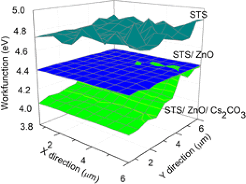
The work functions of various samples (STS, STS/ZnO, STS/Cs2CO3) were mapped on a large scale (6 μm × 6 μm) using a Kelvin probe (Fig. 3). The polished STS substrate exhibited a workfunction of 4.78 eV, whose level in the device is positioned lower than the lowest unoccupied molecular orbital (LUMO) level of Super Yellow emitting layer (−3.2 eV). Such a large energy level difference limits electron injection into the emitting layer and can reduce device efficiency of IPLEDs. Introduction of a ZnO electron injection layer reduced the work function of STS to 4.38 eV. Additionally, the Cs2CO3 electron injection interlayer induced an interfacial dipole and further reduced the work function to 4.08 eV. These reduced work functions decreased the electron injection barrier into the emitting layer from 1.58 eV (STS) to 0.88 eV (STS/ZnO/Cs2CO3) and consequently, can facilitate efficient electron injection into the emitting layer and enable the operation of the devices.
As STS is non-transparent, IPLEDs utilizing STS as both a cathode and substrate require a transparent top electrode to extract the electroluminescence light from the devices. For this purpose, we select a dielectric/ metal/dielectric (DMD) structure (MoO3/Ag/MoO3) as a top electrode, because DMD structures was reported to enhance transparency through the surface plasmon resonance effect within the sandwich structure [10-12].
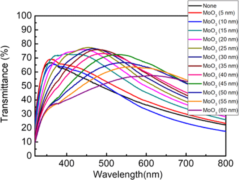
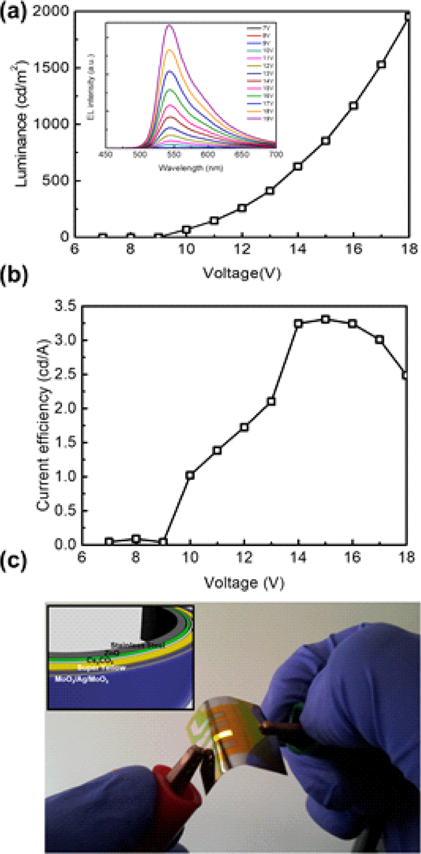
First, we keep the thickness of bottom MoO3 to 5 nm for efficient hole injection into the emitting layer and the thickness of Ag electrode to 15 nm to maintain high electrical current. To find the optimum thickness of the top dielectric MoO3 layer, we measured the transmittance of MoO3 (5 nm)/Ag (15 nm)/MoO3 (x nm) with varying thicknesses of the top MoO3 layer (Fig. 4). The transmittance of the MoO3/Ag/MoO3 increased from ∼42% to ∼70% at 550 nm which is close to the electroluminescence spectrum of the IPLEDs as the thickness of the top MoO3 layer increased to 45 nm, after which it began to decrease (Inset of Fig. 5(a)). Therefore, we selected MoO3 (5 nm)/Ag (15 nm)/MoO3 (45 nm) as the semi-transparent top electrode for the IPLEDs utilizing the STS electrode/substrate (STS/ZnO (22 nm)/Cs2CO3/Super Yellow (∼230 nm)/MoO3 (5 nm)/Ag (15 nm)/MoO3 (45 nm)).
Current efficiency and luminance-versus-voltage characteristics were measured in the devices. The IPLEDs on STS achieved a current efficiency of 3.3 cd/A and a maximum luminance of 2,450 cd/m2 (Fig. 5(a), Fig 5(b)). These IPLEDs utilizing a stainless steel cathode/substrate with the MoO3/Ag/MoO3 transparent top anode demonstrated uniform light emission under bending in ambient air, highlighting the facile flexibility and air stability of our IPLEDs.
4. CONCLUSION
In conclusion, we present the first light-emitting diodes that use metal foils, specifically STS, as both the cathode and substrate. Through the implementation of surface planarization techniques and the incorporation of ZnO electron injection layer, we successfully develop air-stable IPLEDs that use STS as both the cathode and substrate. The introduction of ZnO/Cs2CO3 electron injection layers facilitates efficient electron injection into the emitting layer. Additionally, we optimize the thickness of the top DMD anode to maximize transparency and outcoupling efficiency in IPLEDs. Through a combination of these strategies, we achieved a current efficiency of 3.3 cd/A and a maximum luminance of 2,450 cd/m2. These achievements mark the first reported electroluminescence efficiency of light-emitting diodes that utilize metal foils as both an electrode and a substrate to our best knowledge. Furthermore, this work shows the potential of stable IPLEDs under high temperature and operation because metal foil can dissipate the heat through the conductive substrates [13]. Overall, this work shows the possibility of simplified and cost-effective IPLEDs and pave the way for their practical applications in flexible display and lightings.