
1. INTRODUCTION
Metal halide perovskites have attracted significant attention as next-generation optoelectronic materials owing to their exceptional optical properties, including excellent light-emitting characteristics, narrow full width at half maximum (FWHM), and tunable bandgaps [1-8]. These attributes have driven the rapid development of perovskite light-emitting diodes (PeLEDs), underscoring their technological promise in advanced display applications [9-15].
Despite these advantages, PeLEDs still face substantial stability challenges when exposed to external stimuli such as heat, moisture, and oxygen [16-21]. These limitations originate not only from intrinsic instabilities within the emissive perovskite layer but also from insufficient interfacial compatibility among the various functional layers that constitute the device architecture [22]. Therefore, achieving precise control over the physicochemical properties of all interfaces-particularly the hole transport layer (HTL)-is essential for realizing reliable and high-performance PeLEDs [23,24].
Nickel oxide (NiOx) has emerged as a promising hole transport layer owing to its suitable energy level alignment, high optical transparency, and excellent thermal and chemical stability, even under humid and oxidative conditions [25-27]. However, the surface of NiOx typically exhibits inhomogeneous oxygen vacancies and abundant hydroxyl groups (−OH), which induce interfacial charge asymmetry [28-29]. This results in a surface energy mismatch with the perovskite precursor solution, leading to poor film uniformity, increased interfacial defect density, and ultimately, enhanced non-radiative recombination that constrains device performance [30,31].
A widely adopted strategy to mitigate these interfacial issues involves coating poly (9-vinylcarbazole) (PVK) on NiOx to improve wettability and chemical compatibility [29,32,33]. However, PVK, as a non-polar conjugated polymer, lacks intrinsic molecular polarity, resulting in weak electrostatic interactions and poor adhesion with the ionically polar NiOx and perovskite layers. This polarity mismatch causes surface energy discrepancies that hinder uniform perovskite film formation and promote the formation of interfacial defects.
To overcome these limitations, this study introduces an anionic conjugated polyelectrolyte (CPE), poly [9,9-bis(4-C-sulfonatobutyl)fluorene-alt-thiophene]-Li (PFS-T-Li), as a multifunctional interfacial layer capable of enabling dual passivation at both the NiOx and perovskite interfaces [34-39]. Featuring a conjugated backbone composed of fluorene and thiophene units, PFS-T-Li offers a delocalized π-electron transport pathway that facilitates efficient hole transport. Simultaneously, its sulfonate side chains (SO3−) and Li+ counterions selectively coordinate with oxygen vacancies in NiOx and Pb2+-related trap sites in the perovskite layer, respectively, thereby enabling effective defect passivation and suppressing trap-assisted non-radiative recombination [40-42].
Moreover, the hydrophilic and ionic nature of PFS-T-Li alleviates the surface energy mismatch between NiOx and the perovskite precursor solution, promoting uniform film formation and enhancing interfacial adhesion. By concurrently improving interfacial electronic stability and enabling efficient hole injection, this dual-passivation strategy addresses critical interfacial challenges in PeLED fabrication. Consequently, this study demonstrates that the incorporation of PFS-T-Li represents an effective approach to enhance interfacial compatibility, suppress defect formation, and improve overall PeLED device performance.
2. METHODS
Nickel acetate tetrahydrate (98.0%), ethanol (95.0%), ethanolamine (99.5%), methanol (99.9%), cesium bromide (99.99%), PVK (Mw=1,100,000 g mol−1), chlorobenzene (CB; 99.8%), 18-Crown-6 ether (Crown;≥99.0%), dimethyl sulfoxide (DMSO; 99.9%) 2,7-dibromofluorene (97.0%), potassium hydroxide (90.0%), tetrabutylammonium bromide (98.0%), tetraethylammonium hydroxide aqueous solution (20wt%) and lithium perchlorate (95.0%) were purchased from Sigma-Aldrich, n-Butylammonium bromide (BABr; 99.9%) was purchased from Greatcell Solar Materials. Lead bromide (PbBr2≥98.0%) was purchased from Tokyo Chemical Industry (TCI). 2,2',2''-(1,3,5-benzinetriyl) tris(1-phenyl-1-H-benzimidazole) (TPBi, 99.9%) was purchased from OSM. Lithium fluoride (LiF, 99.9%) was purchased from iTASCO. and 1,4-butanesultone (99.0%), thiophene-2,5-diboronic acid bis(pinacol) ester (97%), tetrakis(triphenylphosphine) palladium (99.9%), were purchased from Fisher Scientific.
The Green quasi-2D PeLEDs were fabricated on an ITO substrate with three different HTL configurations. Device architectures are (1) ITO/ NiOx/quasi-2D perovskite/TPBi/LiF/Al. (2) ITO/ NiOx /PVK/quasi-2D perovskite/TPBi/LiF/Al. (3) ITO/NiOx/PFS-Li/quasi-2D perovskite/TPBi/LiF/Al. The ITO substrates were treated with O2 plasma for 30 minutes. For the preparation of NiOx precursor solution, Nickel acetate tetrahydrate (99.5 mg) was dissolved in ethanol (4 mL) with ethanolamine (24.2 μL) and stirred for 4 hours. The NiOx solution was spin coated on ITO at 4,000 rpm for 40 seconds and annealed at 300°C on hotplate for 1 hour. After annealed, the substrates were transferred into a N2-filled glove box. For NiOx/PVK-based devices, a PVK (4 mg mL−1 in CB) solution was spin-coated onto the NiOx layer at 4,000 rpm for 40 seconds and annealed at 130°C for 10 minutes.
The synthesis of PFS-T-Li was carried out in three steps. First, compound 1 was synthesized by reacting 2,7-dibromofluorene (3.00 mmol, 0.97 g), tetrabutylammonium bromide (0.30 mmol, 96.7 mg), and potassium hydroxide (50 wt%, 5 mL) in DMSO (30 mL) under nitrogen. After stirring at 60°C for 30 min, 1,4-butanesultone (6.60 mmol) was added and the reaction was continued at 60°C for 24 h. The resulting mixture was precipitated in acetone and purified by washing with diethyl ether, followed by recrystallization in ethanol to obtain compound 1 (1.61 g, 80%).
Second, compound 1 (0.4 mmol) was polymerized with thiophene-2,5-diboronic acid bis (pinacol) ester (0.4 mmol) using tetrakis (triphenylphosphine)palladium (0) (10 mol%) as the catalyst in a mixture of degassed DMF (3 mL) and aqueous tetraethylammonium hydroxide solution (20%, 3 mL). The reaction was performed at 95°C for 48 h under nitrogen. The resulting polymer (PFS-T) was purified by dialysis, yielding 83%.
Finally, ion exchange was performed to obtain the lithium form of the polymer. PFS-T was dissolved in methanol and reacted with lithium perchlorate (20 equivalents) at room temperature for 24 h. The polymer was then purified by dialysis to afford PFS-T-Li with a 90% yield. For PFS-T-Li-based devices, a PFS-T-Li solution (0.3 mg mL−1 in methanol) was spin-coated under the same condition (4,000 rpm, 40 seconds) and annealed at 120°C for 15 minutes.
For PFS-T-Li-based devices, a PFS-T-Li solution (0.3 mg mL−1 in methanol) was spin-coated under the same condition (4,000 rpm, 40 seconds) and annealed at 120°C for 15 minutes.
For the NiOx-based devices, no additional layer was deposited on top of the - film. Subsequently, 0.25 M perovskite precursor solution containing PbBr2, CsBr, and BABr in a molar ratio of 1:0.9:1.2 was prepared in 1 mL DMSO with 4 mg of 18-crown-6. quasi-2D perovskite precursor solution spin coated on each HTLs 500 rpm for 5 seconds and 5,000 rpm for 40 seconds and annealed 120°C for 5 minutes. Finally, TPBi (75 nm), LiF (2 nm), Al (100 nm) was deposited via thermal evaporator in 5×10⁻⁶ torr.
The work function values of ITO, ITO/NiOx, ITO/NiOx/PVK, and ITO/NiOx/PFS-T-Li were determined using Kelvin probe microscopy (KPM, KP Technology Ltd., Model KP020). The contact potential difference (CPD) between each sample and the KPM tip was measured to estimate their respective work functions. Prior to measurement, the KPM tip was calibrated using a reference gold surface with a known work function of 5.1 eV. The surface roughness was measured by atomic force microscopy (XE-100, Park System) in contact mode. XPS analysis was determined using a KRATOS Analytical Ltd. (AXIS SUPRA). The PLQY was measured by an absolute photoluminescence quantum yield spectrometer (Quantaurus-QY) from HAMAMATSU with excitation wavelength of 375 nm. UV visible spectra of thin films were determined using a JASCO V-730. The J−V, L−V, EQE-V curves, and electroluminescence features were measured by a Keithley 2,450 source meter with a CS2000 spectroradiometer (Konica Minolta) in a N2 filled glovebox.
3. RESULTS AND DISCUSSION
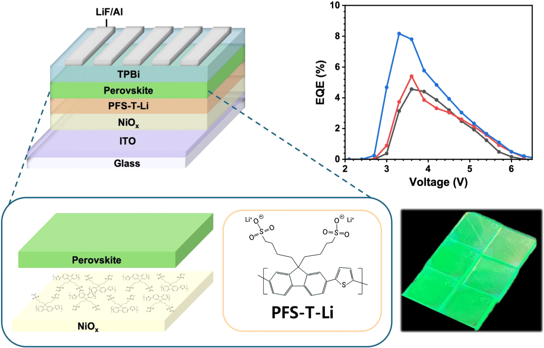
Fig. 1(a) illustrates the chemical structure of CPE, PFS-T-Li, which was designed to function as a multifunctional interfacial layer in PeLEDs. This polymer features a π-conjugated backbone composed of fluorene and thiophene units, providing an extended delocalized π-electron pathway to support hole transport. In particular, in case of thiophene, a planar heteroaromatic ring with high electron density, enhances the π-conjugation between adjacent fluorene units, thereby promoting charge delocalization [35].
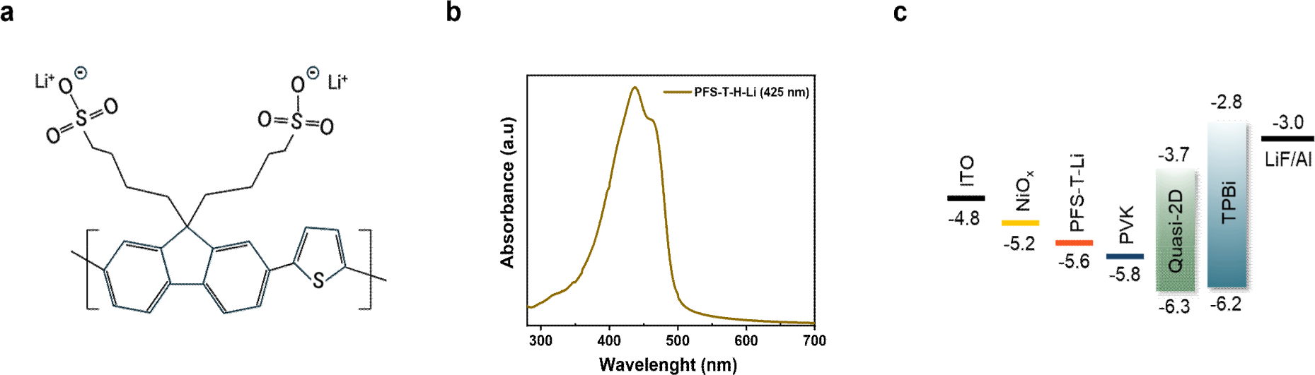
Anionic sulfonate groups (SO3−) are introduced into the side chains and are intended to provide strong electrostatic and coordination interactions at the interface, facilitating robust binding with both NiOx and the perovskite layer. The sulfonyl moieties also allow for charge delocalization, which is expected to stabilize counterions such as Li+. Based on this design, PFS-T-Li is anticipated to exert a dual-passivation effect by targeting oxygen vacancies on the NiOx surface and undercoordinated Pb2+ defects in the perovskite layer.
Leveraging this molecular architecture, PFS-T-Li is intended to act as a multifunctional interfacial layer that enhances hole injection from NiOx to the perovskite by modulating interfacial energy alignment, regulating charge distribution, and passivating interfacial trap states.
In the UV-Vis absorption spectrum, PFS-T-Li exhibits a distinct π-π* transition peak at approximately 425 nm (Fig. 1(b)), attributed to the π-conjugated structure along the polymer backbone, supporting its light-absorbing characteristics as a conjugated polyelectrolyte. This absorption wavelength shows minimal overlap with the emission range of the perovskite layer (510−520 nm), thereby minimizing optical loss upon interfacial insertion. To examine interfacial energetics, the contact potential differences (CPD) of each HTL configuration were measured using the Kelvin probe technique, with the ITO/NiOx film set as the reference. Compared to this baseline, ITO/NiOx/PVK and ITO/NiOx/PFS-T-Li exhibited CPD shifts of −350 mV and −265 mV, respectively (Table S1), indicating downward energy level shifts of the surface Fermi level. This shift reflects the formation of interfacial dipoles and a modified electronic structure that promotes hole extraction. Although the CPD shift induced by PFS-T-Li is slightly smaller than that of PVK, the resulting energy level remains well aligned with the HOMO level of the perovskite (−6.3 eV), forming a cascade alignment across NiOx, PFS-T-Li, and the perovskite layer (Fig. 1(c)). This favorable alignment, together with interfacial defect passivation, facilitates efficient hole injection and lowers the energetic barrier for charge transport.
To quantitatively assess the wettability and interfacial compatibility of ITO/NiOx, ITO/NiOx/PVK, and ITO/NiOx/PFS-T-Li substrates with the perovskite precursor solution, contact angle measurements were performed using the actual precursor solution. This evaluation aimed to probe how effectively each interfacial layer promotes uniform spreading of the precursor and establishes favorable interfacial interactions. Among the tested surfaces, NiOx/PFS-T-Li exhibited the lowest contact angle (10.60°), followed by NiOx (26.68°) and NiOx/PVK (42.24°) (Fig. 2(a)), indicating that PFS-T-Li delivers the highest degree of chemical compatibility with the perovskite solution. This improved affinity is attributed to the ionic and hydrophilic characteristics of the sulfonate side chains, which mitigate the interfacial energy mismatch at the NiOx/perovskite interface.
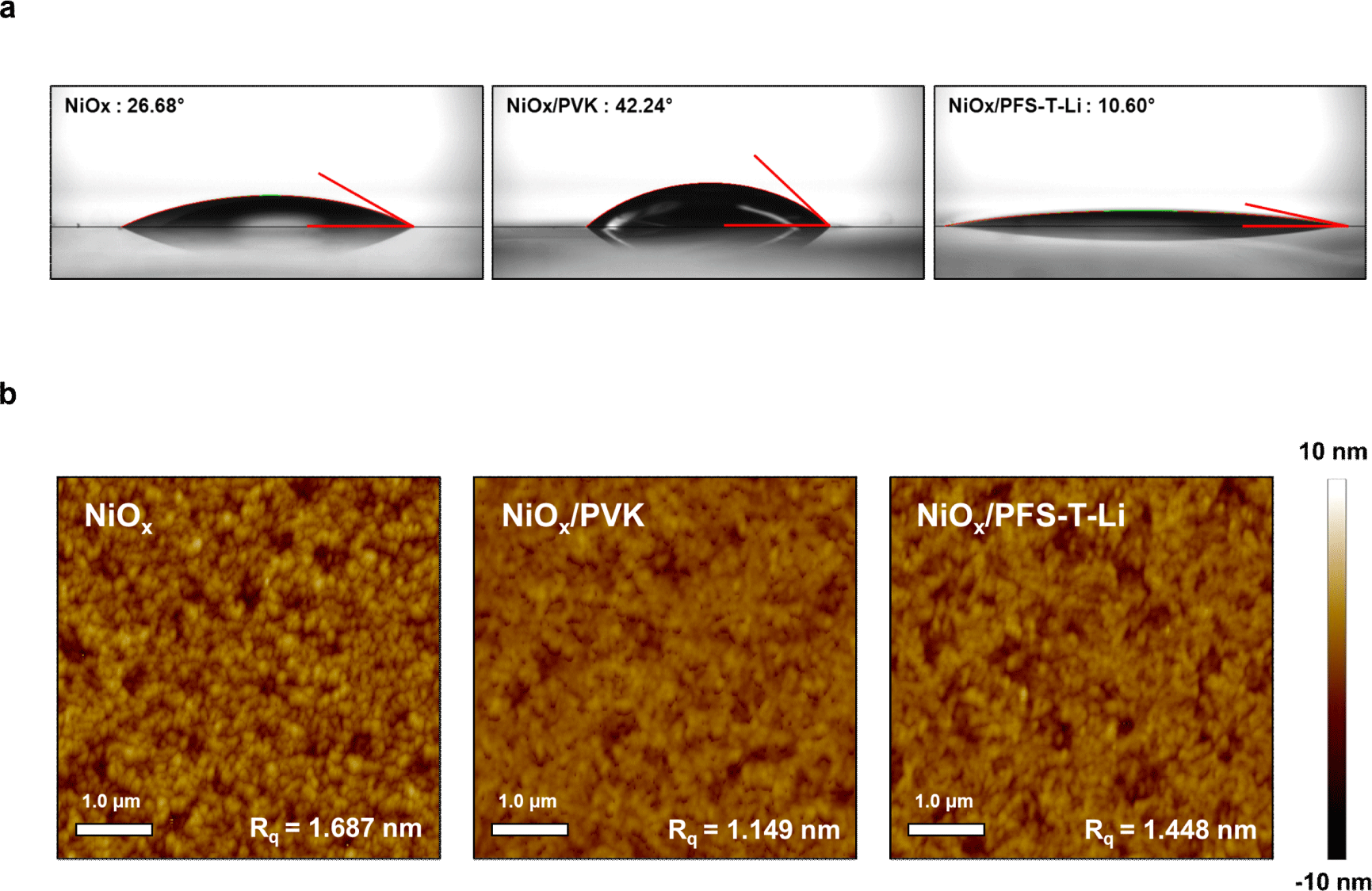
To further investigate the intrinsic surface morphology of the underlying interlayers prior to perovskite deposition, atomic force microscopy (AFM) was conducted (Fig. 2(b)). The pristine NiOx film exhibited a relatively high root-mean-square (Rq) roughness of 1.687 nm, arising from surface inhomogeneities such as oxygen vacancies and residual hydroxyl groups. Upon PVK deposition, the surface roughness decreased significantly to 1.149 nm due to the self-leveling nature of the polymeric film. However, given its nonpolar and chemically inert character, PVK does not chemically interact with or passivate the NiOx surface, as further reflected in its poor wettability with the perovskite solution.
In contrast, the NiOx/PFS-T-Li surface displayed an intermediate Rq value of 1.448 nm, likely attributable to localized structural reorganization induced by electrostatic and coordination interactions between the sulfonate moieties and undercoordinated Ni sites. Notably, the concurrent decrease in contact angle and suppression of surface roughness-despite the absence of a purely smoothing polymer-provides indirect evidence that PFS-T-Li chemically mitigates the surface defect density of NiOx. In particular, the coordination between sulfonate groups and NiOx surface defects is presumed to passivate oxygen vacancies, thereby reducing surface energy inhomogeneity and improving wetting behavior. These synergistic effects are critical for promoting uniform precursor film formation, facilitating nucleation, and ultimately enabling high-quality perovskite crystallization.
To elucidate the interfacial chemical environment, X-ray photoelectron spectroscopy (XPS) was conducted on quasi-2D perovskite films deposited on NiOx and NiOx/PFS-T-Li substrates (Fig 3. (a)–(c)). In the Cs 3d and Pb 4f core-level spectra, the NiOx/ PFS-T-Li sample exhibited discernible downshifts in binding energies by ~0.20 eV and ~0.25 eV, respectively, relative to the pristine NiOx substrate. These shifts reflect a modified local electrostatic environment and reduced interfacial charge accumulation, likely arising from the ionic and coordinating nature of the sulfonate groups SO3− and Li+ counterions, which selectively interact with undercoordinated Pb2+ sites and oxygen vacancies at the NiOx interface. In the Ni 2p core-level spectra (Fig. 3(c)), the NiOx/PFS-T-Li sample exhibited a slight downshift of ~0.05 eV in binding energy relative to the pristine NiOx substrate. This shift suggests a subtle reduction in surface electrostatic interactions, likely due to passivation by the anionic sulfonate groups in PFS-T-Li.
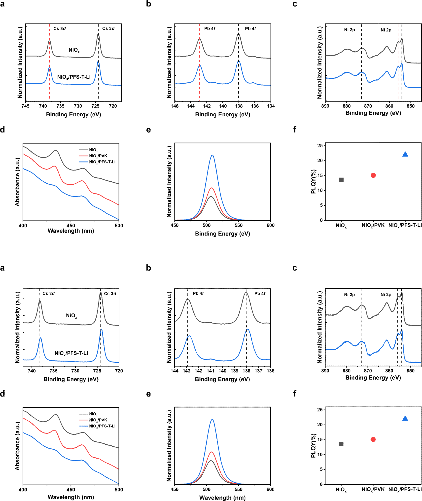
Similarly, no significant shift was observed in the Br 3d spectra (Fig. S1), suggesting that halide ions, which are more tightly bound within the perovskite lattice, remain relatively unaffected by the interfacial modification. The element-specific nature of the observed chemical shifts underscores the selective passivation mechanism, wherein PFS-T-Li preferentially modulates the coordination environment of A-site (Cs+) and B-site (Pb2+) cations rather than lattice halides.
These interfacial interactions contribute to reduced trap-state density and improved charge distribution, supporting more favorable energy level alignment and enhanced optoelectronic performance in the subsequent device operation.
In the UV-Vis absorption spectra (Fig. 3(d)), distinct excitonic peaks at approximately 430 nm and 470 nm, corresponding to the n=1 and n=2 quasi-2D perovskite phases, were observed in all three configurations: NiOx/ perovskite, NiOx/PVK/perovskite, and NiOx/PFS-T-Li/ perovskite. Notably, the peak intensities were substantially reduced in the NiOx/ PFS-T-Li/perovskite sample, suggesting that the incorporation of PFS-T-Li suppresses the relative formation of low-n quasi-2D phases during crystallization. This suppression is attributed to the favorable interfacial environment provided by PFS-T-Li-particularly its ionic sulfonate moieties, which enhance surface wettability and modulate interfacial energetics, thereby directing the growth toward higher-n or more 3D-like perovskite domains. X-ray diffraction (XRD) analysis was conducted to further validate the phase evolution during crystallization (Fig. S2). The peaks at 15° and 30.5° correspond to the (100) and (200) planes of the CsPbBr3 cubic phase, respectively, with the NiOx-/PFS-T-Li/perovskite films exhibiting the highest intensities among all samples. Such enhancement in these main perovskite reflections indicates improved crystallinity, which is attributed to an increased proportion of higher -n phases. The growth of these high-n phases implies a concurrent suppression of low-n phases, leading to a phase distribution shift toward more thermodynamically stable crystal domains [43,44].
This morphological modulation is further supported by photoluminescence (PL) measurements (Fig. 3(e)). The NiOx/PFS-T-Li-based film exhibited the strongest PL intensity among the three configurations, indicating reduced non-radiative recombination losses and enhanced optoelectronic quality. Complementary photoluminescence quantum yield (PLQY) measurements (Fig. 3(f)) revealed a value of 22% for the NiOx/ PFS-T-Li film, representing a significant enhancement over NiOx (13.6%) and NiOx/PVK (15.1%). This finding supports our UV-vis absorption results (Fig. 3d) and is consistent with previous reports showing that reduced low-n phase content improves energy funneling and enhances PL emission efficiency in quasi-2D perovskites [43].
These findings collectively point to a synergistic interfacial passivation effect in the NiOx/PFS-T-Li architecture, where Li+ and SO3− groups selectively interact with Pb2+-related defects in the perovskite and oxygen vacancies in the NiOx, respectively. This dual-passivation mechanism not only mitigates trap-assisted recombination but also promotes more uniform and stable perovskite crystallization. As a result, both the optical emission characteristics and the underlying crystallographic phase distribution are simultaneously improved, laying the foundation for efficient and stable PeLED performance.
To investigate the impact of interfacial engineering on device performance, quasi-2D PeLEDs were fabricated using the structure ITO/HTLs (NiOx, NiOx/ PVK, or NiOx/PFS-T-Li)/perovskite/TPBi/LiF/Al, as illustrated in Fig. 4(a). This device architecture was designed to systematically evaluate how interfacial modifications influence charge injection, recombination dynamics, and overall optoelectronic characteristics. As shown in the current density-voltage (J−V) characteristics (Fig. 4(b)), all devices exhibited typical diode-like behavior. Notably, the NiOx/PFS-T-Li-based device showed a relatively lower current density in the low-bias region (under 3 V), suggesting suppressed leakage current, likely due to effective defect passivation by the sulfonate-functionalized PFS-T-Li layer. At higher voltages within the operational regime, the same device exhibited a markedly higher current density compared to the control (NiOx) and PVK-based devices. This improvement reflects more efficient hole injection, which can be attributed to favorable energy level alignment at the NiOx/PFS-T-Li/perovskite interface and improved interfacial crystallinity, resulting in minimized energetic barriers for carrier transport.
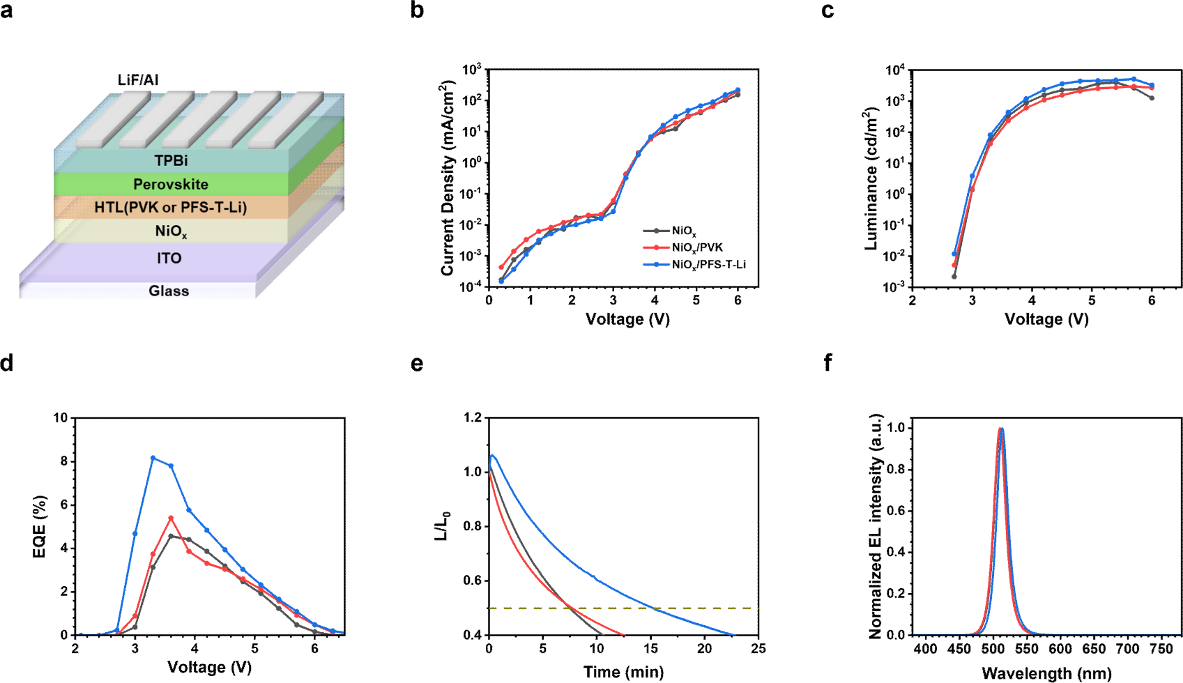
The luminance-voltage (L−V) characteristics (Fig. 4(c)) further support this trend. The device incorporating PFS-T-Li exhibited the highest peak luminance of 5,111 cd m−2, compared to 4,153 cd m−2 and 3,735 cd m−2 for the PVK and bare NiOx devices, respectively. These improvements are consistent with suppressed non-radiative recombination and more balanced carrier injection, resulting from the dual-passivation effects of PFS-T-Li at both the NiOx and perovskite interfaces.
Notably, the device with the PFS-T-Li interlayer also exhibited the highest external quantum efficiency (EQE), reaching 8.16% at 3.3 V (Fig. 4(d)). In comparison, devices with PVK and bare NiOx reached peak EQEs of 5.59% and 4.14%, respectively, at higher voltages. The enhanced performance is attributed to the combined benefits of reduced trap-assisted recombination, improved perovskite film morphology, and better energy level alignment achieved through PFS-T-Li incorporation. The quantitative performance metrics are summarized in Table S2.
Operational stability was evaluated by monitoring the time to 50% initial luminance (T50) under continuous operation at 100 cd m−2 (Fig. 4(e)). The PFS-T-Li-based device exhibited a T50 of 15.2 minutes, approximately double that of the PVK (7.7 minutes) and NiOx (7.5 minutes) devices, underscoring the stabilizing effect of interfacial passivation on device degradation.
Electroluminescence (EL) spectra from all devices exhibited sharp green emission with FWHM values consistently below 20 nm, indicating high color purity regardless of the interfacial layer used. The NiOx and NiOx/PVK-based devices showed peak emission at 510 nm, while the NiOx/PFS-T-Li-based device exhibited peak emission at 513 nm, maintaining emission within the green spectral range.
4. CONCLUSION
In summary, we report a multifunctional interfacial engineering strategy for PeLEDs using an anionic conjugated polyelectrolyte, PFS-T-Li, as an interfacial layer on NiOx-based hole transport layers. The π-conjugated fluorene-thiophene backbone facilitates hole transport, while the sulfonate and lithium moieties simultaneously passivate oxygen vacancies in NiOx and Pb2+-related defects in the perovskite layer. This dual-passivation mechanism improves interfacial compatibility, suppresses non-radiative recombination, and promotes uniform perovskite crystallization. Consequently, devices incorporating the NiOx/PFS-T-Li interlayer exhibit significantly enhanced external quantum efficiency (8.16%) and luminance (5,111 cd m−2), along with improved operational stability. These findings demonstrate the efficacy of PFS-T-Li as an interfacial modulator, offering a viable pathway toward efficient and stable PeLEDs.