
1. INTRODUCTION
Synapses play a crucial role in enabling information transmission within a nervous system [1–5]. The development of electronic devices capable of emulating synaptic information-transition principles is a critical step towards advancing neuromorphic electronics [6–9]. Recently, artificial synapses have been developed using phase change materials, resistive switches, conductive bridges, organic-inorganic halide perovskites (OHP) and semiconductor/ionic gate insulator combinations [10–19]. However, the sensitivity and energy consumption of these devices still require improvement to be comparable with those of biological synapses [20–22].
High sensitivity is especially important for the emulation of peripheral nervous system (PNS) [6,23–25]. In the PNS, sensory nerves play a vital role in converting visual, auditory, and tactile stimuli into electrical impulses, which are then transmitted to the spinal cord. From there, the information is relayed to the central nervous system (CNS) or directly to motor nerves through synaptic connections in the spinal cord, enabling us to exchange information and interact with our environment [26]. The construction of an artificial system that can replicate and potentially integrate with the biological PNS holds significant promise for various fields, including neuroprosthetics and neurorobotics [1,27–32]. This could probably make disabled people to feel their legs or arms again.
However, achieving integration with biological nerves poses challenges, as artificial nerves must be capable of responding to ultralow biological voltage signals, typically around 100 mV [10,11]. This requirement remains a difficult hurdle to overcome. Additionally, in contrast to the CNS, which relies on both short-term and long-term plasticity for information processing, the PNS primarily requires short-term plasticity for fast information transmission while minimizing signal overlap [33]. To attain these goals, new materials, electronic devices and working mechanisms are desired in artificial synapses.
OHP-nanoparticles (NPs) represent a promising class of materials with applications in photovoltaics and light-emitting diodes [34–36]. By modifying the ligands surrounding the NPs, the number of deep traps can be effectively reduced. The presence of alkyl chains in the ligands creates hydrophobic yet amorphous “walls” between the nanocrystallites in the NP thin film, leading to increased resistance in the perovskite films [37]. These walls effectively passivate grain boundaries, known to be the main paths of ion migration [38–40]. Consequently, the hydrophobic walls restrict ion migration within the nanocrystallites, resulting in short-term plasticity being predominantly observed in this device. This characteristic is beneficial for the rapid recovery of synaptic weight after signal transitions in the PNS.
Moreover, OHP-NPs are synthesized in solution, which reduces the film’s dependence on processing conditions and post-treatments compared to OHP polycrystalline thin films. The solution-based process is also potentially compatible with state-of-the-art printing techniques, highlighting the significant potential of OHP-NPs as a new material system in the field of artificial synapses [41]. The unique properties of OHP-NPs, combined with their easy of synthesis and compatibility with scalable manufacturing methods, make them a promising candidate for the advancement of highly sensitive and efficient artificial synaptic devices.
Herein, we report an OHP-NP-based artificial synapse, which can be more suitable for mimicking biological PNS. The artificial synapse is so sensitive that it is functioned at ultralow-voltage down to 100 mV, even comparable with that of biological synapses. Stimulated by pulses at such low voltages, the artificial synapse emulates important working principles of a biological synapse, such as excitatory postsynaptic current (EPSC), paired-pulse facilitation (PPF), spike-rate-dependent plasticity (SRDP) and spike-timing dependent plasticity (STDP). The electronic device could even be stimulated by further reduced external pulses down to 10 mV, and in such a case the device exhibits ultralow energy consumption down to 5 fJ per synaptic event (SE), comparable with that of biological synapses (1–10 fJ/SE). These superior properties benefit from the intrinsic properties of OHP-NPs and their thin films. The high sensitivity and low-energy consumption represent important progress toward ultrasensitive neuromorphic electronics and artificial nerves that interface with biological ones.
2. METHODS
OHP-NPs were synthesized by solubility-difference-induced crystallization methods at room temperature. We prepared the clear perovskite precursor solution by dissolving 0.3 mmol of CH3NH3Br, 0.4 mmol of PbBr2, and 0.6 μmol of n-hexylamine into 5 mL of dimethylformamidinium (DMF). After dripping 1 mL of precursor solution into 5 mL of toluene solution containing 100 μL of oleic acid under vigorous stirring, the solution was centrifuged at 10,000 rpm for 10 min. The supernatant solution was collected to fabricate the synaptic devices.
p+Si wafer was cleaned by sequential sonication in acetone and isopropanol (15 min for each process), boiled in isopropanol, and then blown dried with N2. OHP-NP thin film was spin-coated from solution, and then baked at 90°C for 10 min. Finally, 100-nm-thick circular Al metal dots were thermally evaporated through a shadow mask to define the pixel area of 100 μm2.
Atomic force microscopy (AFM) images were captured using a Dimension 3,100 microscope (Digital Instruments). Scanning transmission electron microscopy (STEM) images were obtained from TEM equipment 2100F with Cs correction. All electrical characteristics of the electronic devices were characterized using a Keithley 4200-SCS semiconductor parameter analyzer in a nitrogen atmosphere.
3. RESULTS AND DISCUSSION
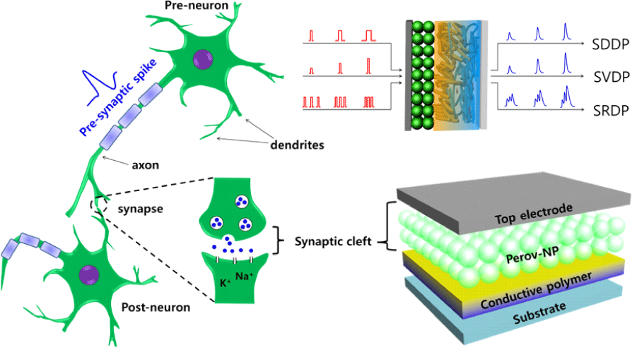
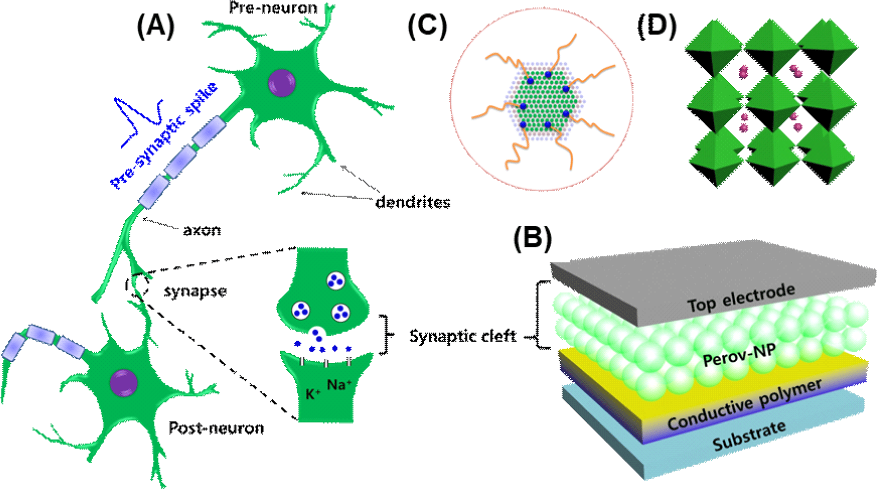
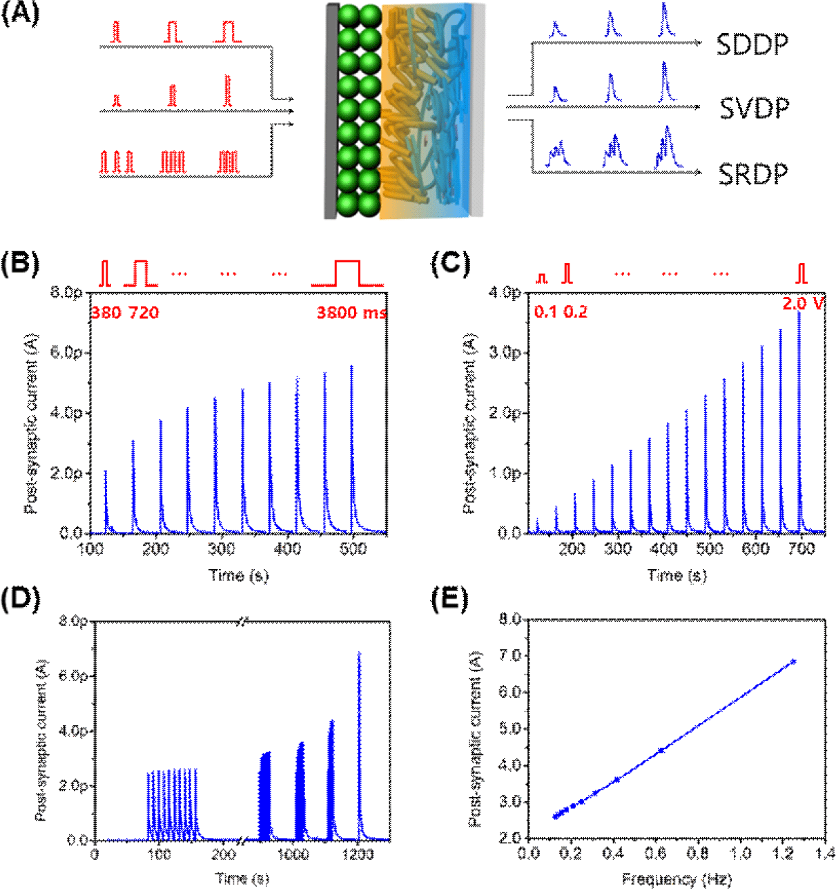
A sandwiched structure of top electrode/OHP-NP/ conductive polymer/p+Si was fabricated to emulate the functions of a biological synapse (Fig. 1A–D). For the conductive polymer, we used polymer composites consisting of PEDOT:PSS (Clevios P VP AI4083) and a perfluorinated ionomer (PFI). This composite layer functions as a reservoir that can trap mobile ions in addition to the insulating surface ligands [20]. The Al top electrode functions analogous to a presynaptic membrane at which presynaptic spikes arrive and trigger the release of neurotransmitters. The sandwiched OHP-NP thin film emulates a synaptic cleft to provide a nanoscale gap to mediate transportation of chemical messengers to modulate synaptic strength. External pulses, i.e., presynaptic spikes, activate ions and induce consecutive ionic migration in the thin film to tune the thin-film resistance, i.e., synaptic strength. Synaptic response was recorded at a constant reading voltage from the bottom electrode that emulates a postsynaptic membrane.
First, we evaluated the size distribution of OHP-NPs used in our artificial synapse. The OHP-NPs were pre-synthesized using methylammonium lead bromide (MAPbBr3) and dispersed in p-xylene. The dispersion was then drop-cast onto polycarbon-coated copper grids and dried. STEM images of the OHP-NPs revealed spherical shapes with diameters ranging from 5 to 10 nm (Fig. 2(A)).
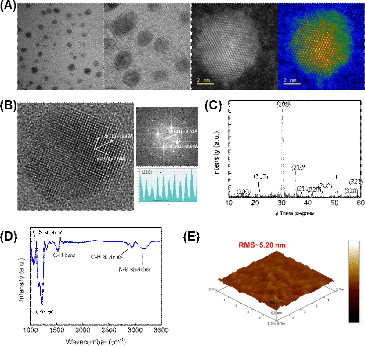
Energy dispersive spectrometry (EDS) mapping and X-ray photoelectron spectroscopy (XPS) further confirmed the successful synthesis of OHP-NPs with Pb and Br elements embedded inside the crystallites (Fig. 2A; SI Figs. 1, 2). The crystal structure within the OHP-NPs was clearly evident from the magnified view of a specific nanocrystallite (Fig. 2B) and was validated using X-ray diffraction (XRD) patterns (Fig. 2C). Fourier-transform infrared spectroscopy (FT-IR) analysis of the perovskite nanoparticles showed characteristic peaks corresponding to C-N stretches (~1,200 cm–1), C-O bends (~1,250 cm–1), C-H bends (~1,500 cm–1), C-H stretches (~2,950 cm–1), and N-H stretches (~3,300 cm–1). These peaks provided evidence of well-adhered ligand chains on the NP surface in film states (Fig. 2D).
Furthermore, AFM imaging revealed a uniform thin film surface, with a root-mean-square roughness of 5.20 nm (Fig. 2E). Overall, our characterization of the OHP-NPs demonstrates their suitability for use in the fabrication of artificial synapses.
An artificial synapse utilizing OHP-NP thin films was fabricated, and the cross-sectional view of the devices confirmed a 15-nm-thick OHP-NP layer in a sandwiched structure (Fig. 3A, Fig. 3B). Synaptic plasticity, which plays a fundamental role in signal transmission in synapses, was investigated by measuring the synaptic weight, modulated by sensorimotor impulses and recovering rapidly during PNS signal transitions. Upon the application of an external pulse, a sudden current shoot is triggered, and after the pulse is removed, it decays within several tens of milliseconds (Fig. 3C), closely resembling the EPSC observed in biological synapses. This phenomenon arises from the redistribution of ions in response to external stimuli, followed by their spontaneous drift back to their original positions. Consequently, this process emulates the arrival of a presynaptic spike on the presynaptic membrane to cause neurotransmitter releasement and the generation of EPSC through the postsynaptic membrane.
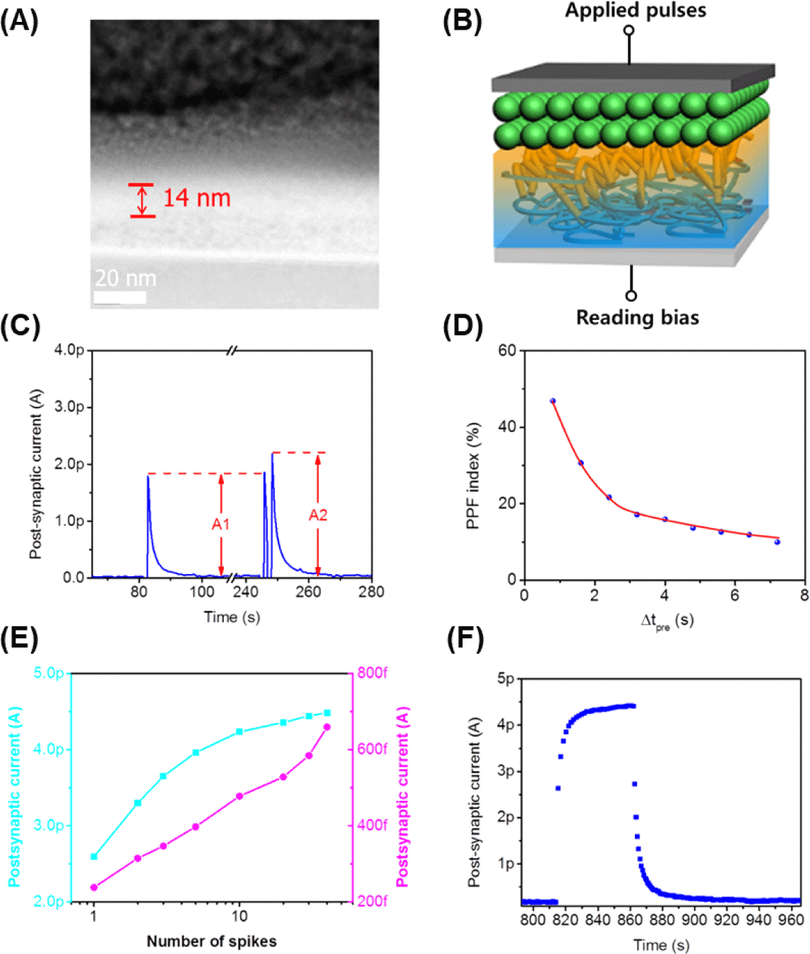
Upon subjecting the artificial synapse to two successive pulses, we observed two EPSC peaks, with the second peak being more intense than the first (Fig. 3C). This behavior closely resembles PPF in biological synapses, a phenomenon underlying various critical brain functions, including information processing and sound localization. The PPF index, representing the incremental percentage of synaptic weight, decreases as the time interval between the two presynaptic spikes increases (Fig. 3D). Remarkably, the PPF index drops to below 10% when the time interval is extended to approximately 7 seconds.
By applying additional consecutive pulses, we observed a gradual step-by-step increase in EPSC amplitude (Fig. 3E, Fig. 3F). This result suggests that ion migration during these spiking periods occurs faster than their recovery. In MAPbBr3 perovskites, Br− exhibits a lower activation energy for ion migration (≈0.2 eV) compared to MA+ and Pb2+ (both≈0.8 eV). Therefore, we consider that Br− ions predominantly contribute to the ion migration and the modulation of synaptic strength in our system. We have seen that both maximal EPSC (Cyan) and EPSC (10 s after stimuli, Magenta) gradually increase with increasing spike number (Fig. 3E, Fig. 3F).
In order to demonstrate the diverse synaptic functions of our artificial synapses based on OHP-NPs, we conducted measurements of EPSC peaks while varying the intensity of spike duration (spike-duration-dependent plasticity (SDDP), Fig. 4A, Fig. 4B), the spike amplitude (spike-voltage-dependent plasticity (SVDP), Fig. 4C), and the spike rate (SRDP, Fig. 4D). The artificial synapses utilizing OHP-NPs exhibited gradual increases in EPSC peaks with increasing spike duration, spike amplitude, and spike rate, demonstrating the versatility and adaptability of the artificial synapse in response to different spiking patterns and durations. Particularly, the spike rate and frequency demonstrated a linear relationship with EPSC peaks (Fig. 4E).
Next, we investigated STDP, a crucial form of the Hebbian learning rule, which posits that “neurons that fire together, wire together” [42]. STDP describes the modulation of synaptic weight when the relative timing between presynaptic and postsynaptic spikes is changed. To evaluate the applicability of STDP in our artificial synapses, we applied a series of pulse pairs to the presynaptic and postsynaptic terminals and recorded the changes in postsynaptic current. We observed an anti-symmetric plot of STDP (SI Fig. 3A, Fig. 3B), consistent with the biological phenomenon where synapses typically strengthen when presynaptic spikes precede postsynaptic spikes, while the reverse sequence leads to synaptic depression.
To study the sensitivity and energy consumption of the synaptic devices, presynaptic spikes with various amplitudes were applied and concomitant EPSC was recorded (Fig. 4C). Remarkably, the device exhibited exceptionally high sensitivity, successfully realizing all the aforementioned functions with stimuli applied at a voltage level as low as 100 mV. Furthermore, the electronic device demonstrated the ability to respond to even smaller presynaptic spikes, as low as 10 mV. This sensitivity level represents one of the highest among state-of-the-art two-terminal synaptic devices, surpassing that of a biological synapse, where action potentials of approximately 70 mV are typically applied. Such high sensitivity is crucial for the development of bio-integrating electronics, enabling the detection of weak signals at the bio/electronics interface, and represents a significant step towards constructing ultrasensitive neuromorphic electronics for brain-inspired applications.
The human brain remarkably functions at a power level comparable to that of a household lightbulb, despite its billions of neurons and trillions of synapses. This energy efficiency is primarily due to the low power consumption of synapses, typically in the range of 1–10 fJ per SE. Consequently, for the construction of a truly energy-efficient artificial system, low-energy consumption by artificial synapses is a critical requirement. Our calculations based on the pulse amplitude (A), the triggered current (I), and the pulse width (t) of the EPSC peak, triggered by a 10–mV pulse, revealed an extremely low energy consumption of approximately 5 fJ per SE. This energy consumption level represents one of the lowest observed among two-terminal synapse-emulating electronic devices to date and is comparable to that of a biological synapse [6,20]. Furthermor7, these values are comparable with those of other two- or three-terminal synaptic devices (~10 fJ/synaptic event) in previously reported literature [43]. These findings demonstrate the significance of the high sensitivity and remarkably low energy consumption for the development of an exceptionally sensitive and energy-efficient artificial neural system. With such capabilities, our artificial synapses based on OHP-NPs hold great promise for advancing neuromorphic computing and brain-inspired technologies.
4. CONCLUSION
In conclusion, we have successfully fabricated an OHP-NP-based artificial synapse capable of emulating crucial synaptic functions, including short-term memory, spike-timing dependent plasticity, and spike-rate dependent plasticity, all in response to stimuli as low as 100 mV. The remarkable sensitivity of this device places it in the same order as biological synapses, making it highly promising for applications in bioinspired and bio-integrated artificial nervous systems. These exceptional electronic properties are attributed to the unique nanostructure of OHP-NPs and their thin films, which confine ion migration within nanocrystallites, resulting in ultrasensitive responses and rapid recovery of synaptic weight. Ultimately, these breakthroughs may lead to the realization of highly sophisticated and efficient bio-inspired artificial intelligence systems with a wide range of practical applications in the fields of neuroscience, robotics, and medical prosthetics.