


1. INTRODUCTION
Organic thin-film transistors (OTFTs) have attracted significant attention as promising candidates for next-generation flexible, low-cost, and large-area electronic applications [1-8]. However, achieving low operating voltages and high performance simultaneously remains a critical challenge, largely limited by the dielectric layer's properties and the organic semiconductor/dielectric interface [9-12]. Furthermore, the interfacial properties between the organic semiconductor and dielectric critically influence charge transport and overall device performance. Engineering and optimizing these interfaces are essential to realize high-performance OTFTs with stable and efficient operation [9-12]. Extensive efforts have been devoted to enhancing OTFT performance, particularly by achieving low-voltage operation through diverse processing strategies [13-24]. Conventional low-k dielectric materials such as silicon dioxide (SiO2), with a dielectric constant of ~3.9 [18,24], inherently limit gate capacitance at a given thickness, thereby requiring high operating voltages that are unsuitable for low-power applications. On the other hand, integrating high-k dielectrics such as aluminum oxide (Al2O3), with a dielectric constant between 6 and 9 [18, 24], provides a promising approach to overcome these limitations by increasing gate capacitance, thereby reducing operating voltages and improving charge modulation [18,24]. While high-k Al2O3 is widely used in inorganic electronics [21,22], its application in OTFTs remains limited, particularly in configurations that avoid complex surface treatments. This is largely due to the sensitivity of organic semiconductors to interfacial disorder, which can introduce trap states and degrade device performance. This gap highlights the need to investigate simplified high-k dielectric strategies that ensure favorable interface characteristics while enhancing OTFT performance. In this regard, engineering bilayer dielectric stacks by integrating high-k Al2O3 atop SiO2 offers a promising route to improve dielectric function and interfacial compatibility without relying on surface modifications or self-assembled monolayers (SAM). This approach may enable high-performance, low-power p- and n-type OTFTs for future flexible and wearable electronics.
Herein, we systematically investigate the effect of integrating a high-k Al2O3 layer into the gate dielectric stack on hole and electron transport in OTFTs. We directly compare devices using conventional low-k SiO2 and high-k Al2O3/SiO2 bilayers, with p-channel pentacene and n-channel N, N′-dioctyl-3,4,9,10-perylenedicarboximide (PTCDI-C8) as the active layers. ll transistors were fabricated and characterized without any surface treatments or self-assembled monolayers (SAM) on the dielectric surface to investigate the intrinsic nature of Al2O3. Our detailed evaluation of a 20-nm Al2O3 layer shows significant improvement in electrical performance for both charge carrier types. In particular, devices with the Al2O3/SiO2 bilayer operate within ±10 V and exhibit markedly enhanced key device parameters compared to those with SiO2. This dielectric engineering approach offers a clear pathway to low-power, high-performance OTFTs by increasing the dielectric constant and improving the semiconductor/dielectric interface.
2. MATERIALS AND METHODS
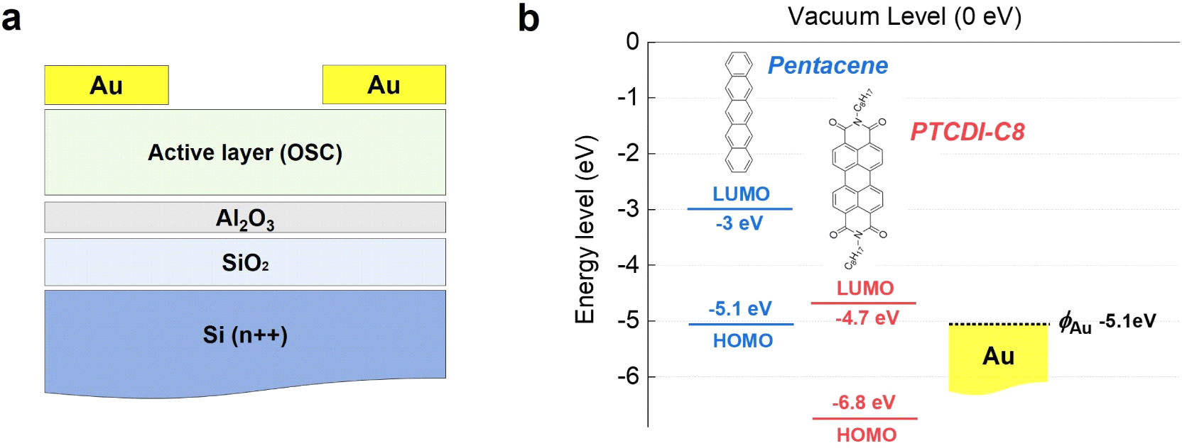
All chemicals used in this study were purchased from Sigma-Aldrich and used without further purification. The schematic cross-section of the bottom-gate, top-contact OTFT structure fabricated in this work is shown in Fig. 1(a). The energy levels, including the Fermi level of Au, and the HOMO and LUMO levels of pentacene and PTCDI-C8, along with the molecular structures of pentacene and PTCDI-C8, are shown Fig. 1(b). OTFTs were fabricated on heavily n-doped Si wafers serving as both the substrate and gate electrode, coated with a 200 nm thermally grown SiO2 gate dielectric. Prior to organic layer deposition, substrates were ultrasonically cleaned in acetone, isopropanol, and deionized water, followed by UV/ozone treatment (20 min) and nitrogen drying (5 min). Two gate dielectric configurations were employed: a single-layer low-k SiO2 (200 nm) and a bilayer high-k Al2O3 (20 nm)/low-k SiO2 (200 nm). For the bilayer structure, a 20 nm Al2O3 layer was deposited by atomic layer deposition (ALD) atop the SiO2 dielectric, which served as the initial dielectric layer. The ALD process was conducted at 150℃ using trimethylaluminum (TMA) as the metal precursor and water vapor as the oxidant. Depositions proceeded through alternating, self-limiting exposures to TMA and H2O, resulting in a growth rate of approximately 1.1 Å per cycle. Pentacene and PTCDI-C8 were thermally evaporated as p- and n-type organic semiconductors, respectively, at 0.05 nm/s under 5×10⁻⁶ mbar vacuum, to a thickness of 50 nm. Gold (Au) source and drain (S–D) electrodes (80 nm) were then deposited through a shadow mask, defining a channel length (L) of 50 μm and width (W) of 2,000 μm. All electrical characterizations of the OTFTs were conducted in the dark under vacuum (~10−1 mbar) using a Keithley HP 5156 semiconductor characterization system.
3. RESULTS AND DISCUSSION
Table 1 summarizes the dielectric type, dielectric constant, capacitance per unit area, bandgap energy, and thickness of each gate dielectric [18,24]. The equivalent total capacitance of the Al2O3/SiO2 bilayer dielectric was calculated using the series capacitance model according to:
where the individual areal capacitances of Al2O3 and SiO2 are given in Table 1. Based on this relation, the equivalent capacitance Ceq of the bilayer dielectric was calculated to be approximately 7.9 nFcm−2.
Fig. 2(a)–(b) shows the transfer characteristics (Id–Vg) and transconductance (gm) as a function of Vg in the linear regime for p-channel (Vd=–10 V) and n-channel (Vd=+10V) OTFTs with SiO2 gate dielectric, respectively. Meanwhile, Fig. 2(c)–(d) displays the corresponding characteristics for p-channel (Vd=–1 V) and n-channel (Vd=+1 V) OTFTs with Al2O3 (20 nm)/SiO2 (200 nm) bilayer gate dielectric, respectively. As shown in Fig. 2(a)–(d), a clear difference in device performance is observed between p- and n-channel OTFTs with SiO2 (200 nm) and those with Al2O3 (20 nm)/SiO2 (200 nm) bilayer dielectric.
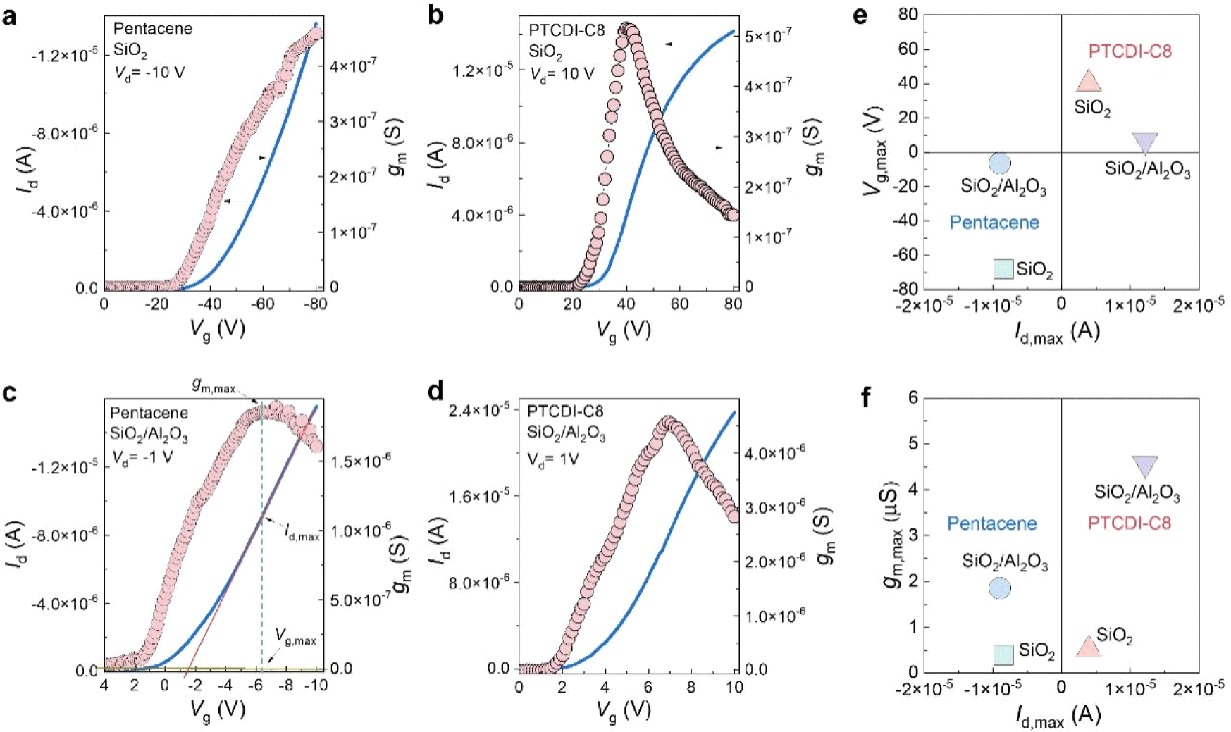
Devices with SiO2 required higher operating voltages and exhibited lower drain currents. In contrast, incorporating a 20 nm Al2O3 interlayer significantly enhanced the drain current, reaching−1.55×10⁻⁵ A for p-channel and 2.37×10⁻⁵ A for n-channel devices at relatively low voltages.
Transconductance (gm), which quantifies the modulation of Id as a function of Vg at a constant Vd, is calculated using [25,26]:
where µlin is the linear mobility, Ci is the capacitance of the insulator per unit area, and W and L represent the channel width and length, respectively.
To ensure a fair device performance comparison, the extrapolation in the linear region (ELR) method [27,28] was employed to extract the maximum drain current (Id, max), the gate voltage at peak transconductance (Vg,max), and the maximum transconductance (gm,max) from the transfer and transconductance characteristics in the linear regime of each device, as illustrated in Fig. 2(c). The extracted values of Vg, max and gm, max are plotted as a function of Id, max in Fig. 2(e)–(f). Interestingly, both p- and n-channel OTFTs with a Al2O3/SiO2 dielectric exhibited significantly higher gm, max values, 1.2×10⁻⁶ S (p-channel) and 8.6×10⁻⁷ S (n-channel), under low Vg, max, compared to 5.2×10⁻⁸ S and 5.4×10⁻⁷ S, respectively, for devices with SiO2, confirming the enhanced performance.
These behaviors are mainly attributed to the enhanced charge storage capability at the conductive channel/dielectric interface, where the Al2O3/SiO2 bilayer enables efficient charge carrier accumulation at low operating voltages, leading to increased Id and gm.
Furthermore, the measured gm increases quasi-linearly with Vg and decreases at high Vg, as can be seen in Fig. 2(b)–(d). Presumably, the decrease in gm at high Vg results from the presence of contact resistance (Rc) at the S–D electrodes/organic semiconductor interface [25, 29].
Fig. 3(a)–(d) presents the transfer characteristics (Id–Vg, left axis) and the square root of the drain current versus gate voltage (–Vg, right axis) in the saturation regime for both p-channel and n-channel OTFTs. The comparison includes devices with a SiO2 dielectric operated at ±80 V and those with an Al2O3/SiO2 bilayer dielectric operated at ±10 V. As shown in Fig. 3(c)–(d), both p-channel and n-channel OTFTs incorporating the Al2O3/SiO2 bilayer operate reliably at a low voltage of ±10 V, attributed to the high dielectric constant of the inserted Al2O3 layer. In contrast, devices with SiO2 alone require a higher operating voltage (±80 V) to achieve similar electrical performance. A maximum Id level of −3×10⁻⁵ A at −10 V was achieved for the p-channel OTFT, while the n-channel device exhibited 3.75×10⁻⁵ A at +10 V, both employing the Al2O3/SiO2 bilayer dielectric. In contrast, at the same operating gate voltages (−10 V for p-channel and +10 V for n-channel), devices with SiO2 exhibited significantly lower drain currents of −2.6×10⁻⁵ A and 1.84×10⁻⁵ A, respectively.
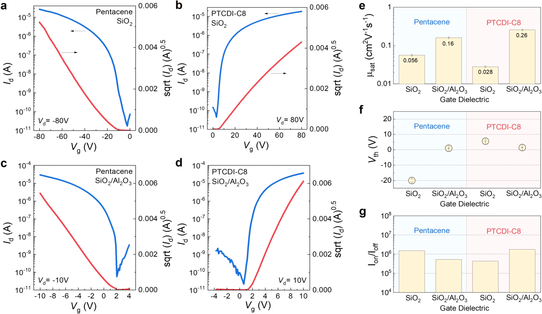
It can be concluded that the use of an Al2O3 interlayer on SiO2 effectively enables high saturation current operation at low voltage for both p-channel and n-channel OTFTs, outperforming devices with SiO2.
In the saturation regime, the mobility is extracted using the following equation [25,26]:
The threshold voltage (Vth) for each device was extracted by linearly fitting the square root of the transfer characteristics in the saturation regime and extrapolating to zero drain current.
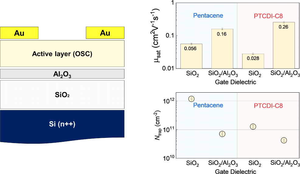
The maximum saturation mobility values (µsat, max) for all devices are shown in Fig. 3(e), while the obtained Vth values are presented in Fig. 3(f). As shown in Fig. 3(e), the highest mobility values were obtained from devices with the Al2O3/SiO2 bilayer dielectric, reaching 0.26 cm2 V−1 s−1 for n-channel and 0.16 cm2 V−1 s−1 for p-channel OTFTs, compared to 0.028 and 0.056 cm2 V−1 s−1, respectively, for devices with SiO2.
Devices employing a Al2O3/SiO2 bilayer dielectric exhibit near zero Vth, measured at approximately 1.0 V for p-channel and 1.46 V for n-channel OTFTs, in contrast to devices with a SiO2 dielectric, which show significantly higher Vth values of −20 V and 5.6 V, respectively. Such low Vth is crucial for the integration of OTFTs into low-voltage circuits [30]. The observed difference in Vth between SiO2-based and Al2O3/SiO2-based devices underscores the strong influence of dielectric composition on device behavior.
The current on/off ratios (Ion/Ioff) for all devices are also extracted from the Id–Vg characteristics in the saturation regime and are presented in Fig. 3(g). Among all devices studied, the n-channel transistor with a 20-nm Al2O3 insertion layer exhibits the highest Ion/Ioff ratio of 1.736×10⁶, significantly improved compared to the device with SiO2, which shows a ratio of 4.263×10⁵.
In contrast, the p-channel device shows a decrease in Ion/Ioff when Al2O3 is incorporated atop SiO2.
Next, the turn-on voltage (Von) refers to the gate voltage at which a conductive channel begins to form between the S–D electrodes [31]. Fig. 4(a) shows the measured values of Von for all devices. Remarkably, all the Von values were notably low, suggesting a better gate voltage modulation. Therefore, the low Von values observed in our p- and n-channel OTFTs are advantageous and comparatively lower than those previously reported in other OTFTs [28,32].
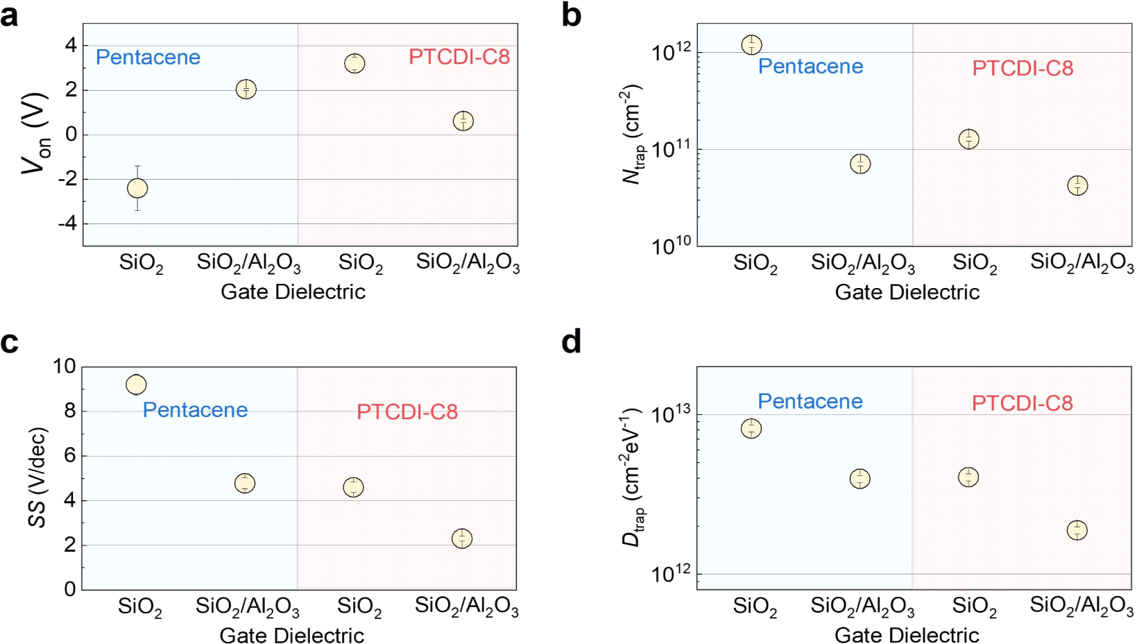
The enhanced performance of both p- and n-channel OTFTs is attributed to the improved interfacial properties introduced by the high-k Al2O3 layer, along with the advantage of its high dielectric constant, which enhances electrostatic control and enables lower operating voltages. This high-k layer likely reduces the interfacial trap density, resulting in higher drain current, enhanced saturation mobility, and reduced Vth, and Von. To further investigate this effect, interface trap densities were systematically extracted for all devices across both lower and higher energy regions.
In OTFT devices, the trap density at the dielectric/ OSC interface, along with structural disorder in the semiconductor, is often suggested to influence the Vth, Von, and SS [33,34]. Here, two independent approaches were employed to estimate the trap densities associated with each dielectric layer.
The first approach estimates the interfacial trap density (Ntr) based on the measured Vth and Von, providing insight into trap-related interfacial characteristics, as given by the following equation [35]:
The calculated Ntr values are presented in Fig. 4(b). Notably, the highest extracted trap state densities (Ntr) were 1.2×1012 cm−2 for p-channel and 1.275×1011 cm−2 for n-channel OTFTs employing SiO2 as the gate dielectric. In contrast, the lowest Ntr values were 7×1010 cm−2 for p-channel and 4.23×1010 cm−2 for n-channel devices with the Al2O3/SiO2 bilayer. These results indicate that both p- and n-channel OTFTs with Al2O3/SiO2 dielectrics exhibit low trap state densities near to the Fermi level [36], corresponding to the low-energy region.
In this second approach, the interface trap density (Dit) is extracted from the SS values using the following expression [29, 35]:
where T is the temperature, k is Boltzmann’s constant, q is the elementary charge, and SS is the subthreshold swing. SS serves as a key indicator of device performance and is directly influenced by the trap density at the organic semiconductor (OSC)/gate dielectric interface. It can be extracted from the transfer characteristics using [29]:
The calculated SS and Dit values are presented in Fig. 4(c), Fig. 4(d), respectively. Although the second method also examines trap states near the Fermi level, it is mainly used to extract the trap state density per unit energy at higher energy levels beyond the range covered by the first method. Fig. 4(d) shows relatively high interface trap densities at higher energy levels, with values of 8.15×1012 cm−2 eV−1 (p-channel) and 4.05×1012 cm−2 eV−1 (n-channel) for SiO2 devices, which are reduced to 3.95×1012 cm−2 eV−1 and 1.88× 1012 cm−2 eV−1, respectively, in devices using the Al2O3/ SiO2 bilayer. These findings indicate that the differences in electrical performance are primarily influenced by deep trap states located closer to the highest occupied molecular orbital (HOMO) in p-channel devices and the lowest unoccupied molecular orbital (LUMO) in n-channel devices, suggesting that trap states in the high-energy region have a greater impact than those in the low-energy region.
Fig. 5(a), Fig. 5(b) shows the output characteristics (Id–Vd) of p-channel and n-channel OTFTs with a SiO2 gate dielectric, while Fig. 5(c), Fig. 5(d) displays the corresponding characteristics of devices employing an Al2O3/SiO2 bilayer dielectric. As shown in Fig. 5(c), Fig. 5(d), the incorporation of a 20 nm high-k Al2O3 layer enables both p- and n-channel OTFTs to operate at low voltages (±10 V), compared to the higher voltage requirements of devices using SiO2. All devices exhibit a clear transition from the linear to the saturation regime, where Id increases linearly at low Vd and saturates at higher Vd due to channel pinch-off. The introduction of the Al2O3 layer enhances the Id level at low applied drain and gate voltages, as evidenced by the output characteristics. This result further confirms that the Al2O3/SiO2 bilayer dielectric improves the semiconductor/dielectric interface, facilitating more efficient charge transport and leading to higher Id levels.
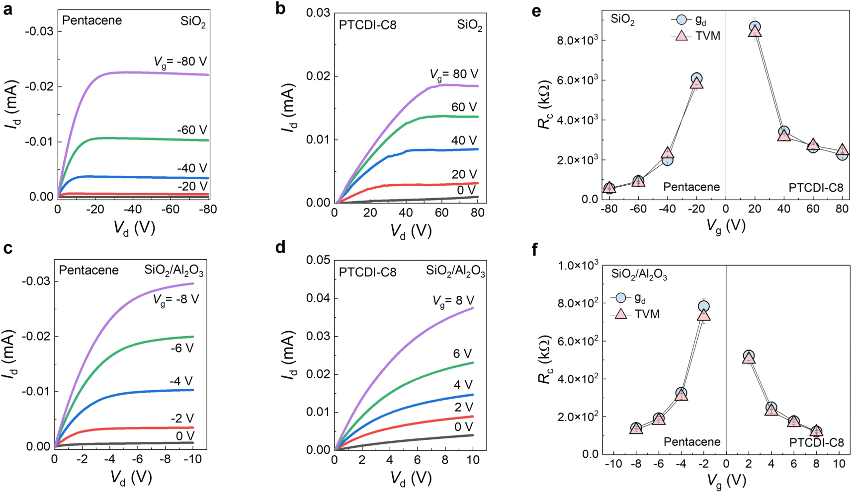
Rc can significantly hinder charge injection, thereby limiting the overall performance of OTFTs [28,37,38]. Understanding its impact on carrier injection from the S–D electrodes to the conductive channel is essential for optimizing device efficiency. Several methods have been developed to extract Rc, including the Y-function method, the transfer line method (TLM), the transition voltage method (TVM), and the output conductance method [28,37,38]. Herein, the influence of the dielectric on contact resistance was assessed using two complementary methods: the transition voltage method (TVM) and the conductance method, both of which were employed to accurately extract Rc of the investigated OTFTs.
At low drain voltage, the output conductance of the devices can be expressed as follows [39]:
For each device and at each Vg, the total source–drain resistance (Rtot) is extracted from the slope of the linear region of the Id–Vd output curve, using
Rc can be extracted as follows:
In addition, an alternative method to extract Rc is the transition voltage method (TVM), where it is expressed as follows [28]:
Where, Vtr is the transition voltage from linear to saturation regime in the output characteristics, and Isat is the saturation drain current. At a given Vg, Vd=Vtr and Ilin=Isat. The Vtr and Isat values are derived from the intersection of the two slopes in the linear and saturation regimes of the output characteristics. The extracted Rc values of all p- and n-channel OTFTs with SiO2 and Al2O3/SiO2 bilayer dielectrics are plotted as a function of VG in Fig. 5(e)–(f), respectively. Notably, the Rc values obtained from both methods show a good agreement, underscoring the reliability of the analysis, as demonstrated in Fig. 5(e)–(f). The extracted Rc values at high VG=±80 V for OTFTs employing SiO2 as the gate dielectric are 5.68×10² kΩ for the p-channel pentacene device and 2.25×10³ kΩ for the n-channel PTCDI-C8 device. Upon introducing a 20 nm high-k Al2O3 layer atop the SiO2 dielectric, Rc values decrease substantially for both device types. For the p-channel device, Rc is reduced to 1.4×10² kΩ, while the n-channel device shows a further decrease to 1.2×10² kΩ, both measured at VG=±8 V. Under these conditions, both devices exhibit comparable Rc values. The reduction in Rc observed in devices with Al2O3/ SiO2 compared to those with SiO2 alone is likely attributed to a lower trap density at the semiconductor/ dielectric interface, which promotes more efficient charge carrier transport owing to the beneficial influence of the additional high-k Al2O3 layer.
The comparative analysis of electrical characteristics of both p-channel and n-channel OTFTs with SiO2 and Al2O3/SiO2 gate dielectrics reveals a consistent and compelling trend of performance enhancement across all metrics, underscoring the effectiveness of the bilayer dielectric strategy. Devices employing the Al2O3/SiO2 bilayer exhibit superior performance, marked by higher µsat, steeper SS, lower trap densities, and reduced Rc compared to their SiO2 counterparts. These improvements are mainly attributed to the dual benefits of the high-k Al2O3 layer: (i) enhanced electrostatic control due to the increased dielectric constant, which enables efficient charge carrier accumulation at low operating voltages, and (ii) a reduction in interface trap states at the semiconductor–dielectric interface, facilitating more efficient charge transport. Importantly, these enhancements were achieved without any surface treatments or SAMs, underscoring the intrinsic ability of high-k Al2O3 to form a favorable and trap-minimized interface with organic active layers. These results further underscore the effectiveness of this dielectric engineering strategy in advancing low-power, high-performance organic electronics.
4. CONCLUSION
In summary, p-channel pentacene and n-channel PTCDI-C8 OTFTs were fabricated using either a SiO2 dielectric or Al2O3/SiO2 bilayer. The bilayer dielectric effectively lowers the operating voltage to ±10 V while improving charge transport, thereby significantly enhancing overall device performance. Devices with Al2O3/SiO2 show improved mobility (0.16 cm2V−1s−1 for holes and 0.26 cm2V−1s−1 for electrons), higher transconductance, near-zero Vth and Von, and higher on/off current ratios. The Al2O3 layer also significantly lowers Rc (1.4×10² kΩ for p-channel and 1.2×10² kΩ for n-channel) and trap densities. These improvements are mainly attributed to the dual benefits of the high-k Al2O3 layer, which enhances electrostatic control through its higher dielectric constant, enabling lower operating voltages, and simultaneously reduces interface trap states at the semiconductor/dielectric interface, facilitating more efficient charge transport. Together, these findings highlight the importance of dielectric interface engineering for improving both p- and n-type OTFT performance and enabling energy-efficient, low-power organic electronics.