
 PDF Download
 PubReader
 Export Citation
 Email the Author
 Share Facebook
 Share Twitter
 Cited by 0 Article
 Metrics (View:1,208)






1. INTRODUCTION
With advances in information technology, electronic devices have become increasingly integrated into nearly all aspects of daily life, driving the evolution of device form factors toward more flexible configurations [1–4]. In addition, with the growing prominence of physical artificial intelligence, the development of intelligent electronic devices capable of stable operation under dynamic conditions has accelerated, thereby increasing the demand for devices that can maintain reliable performance under mechanical deformation [5–8]. In this regard, flexible transparent conducting electrodes (TCEs) play an important role in optoelectronic devices, displays, and sensors, where they are required to maintain optical transmittance and low sheet resistance under mechanical deformation [9,10]. Although conventional indium tin oxide (ITO) electrodes offer high optical transmittance and low sheet resistance, their inherent brittleness limits their use in flexible devices [11,12]. Therefore, research efforts have been directed toward the development of alternative materials and structural designs for flexible TCEs.
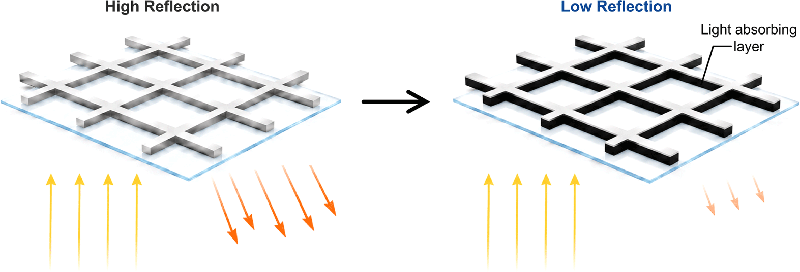
Material-based approaches, including conductive polymers, metal nanowires, graphene, and carbon nanotubes (CNTs), have been proposed; however, their performance as TCEs is limited by low electrical conductivity, high junction resistance, and poor network connectivity [13–15]. As an alternative strategy, structure-based designs that address the trade-off between optical transmittance and electrical conduction have been explored. For instance, ultrathin metal configurations can improve optical transmittance, but strong optical absorption and discontinuous growth behavior limit achievable transparency [16,17]. Alternatively, patterning metals into open structures, particularly metal mesh configurations, has attracted attention as an effective approach to enhance transmittance while maintaining low sheet resistance [18–20]. However, due to the inherently high reflectivity of metals, metal mesh-based TCEs suffer from reduced visibility in bright environments and the noticeable appearance of electrode patterns. This issue arises mainly from reflection at the metallic line region, whereas the surrounding open areas are intended to maintain optical transparency. Therefore, an effective reflection-reduction strategy should target the metal-line region selectively, without covering the transparent area or altering the conductive metal network.
In this study, we introduce a flexible metal mesh TCE incorporating a localized black polyimide (BPI) light absorption layer to reduce metal-induced reflection. The BPI layer, consisting of carbon- black-dispersed polyimide, was patterned via thermal imprinting, Ag nanoparticle (NP) ink filling, thermal treatment, and selective etching, thereby self-localizing the light-absorption layer beneath and near the Ag mesh lines. This structure was designed to lower the apparent reflectance of the reflective metal-line region while preserving the essential electrical and optical characteristics required for transparent electrodes. The reflectance reduction was evaluated from the Ag electrode region, where metal-induced reflection primarily occurs. In addition, the sheet resistance and optical transmittance of the fabricated electrode were examined to assess the feasibility of localized BPI integration as a route toward low-reflectance flexible metal mesh electrodes.
2. METHODS
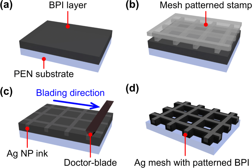
Ag NP-based ink was selected for the fabrication of metal mesh electrodes due to its oxidation stability and electrical conductivity [21]. To enable application on flexible film substrates via low-temperature sintering, the particle size was kept below 200 nm, and polygonal NPs were employed to increase interparticle contact area, thereby improving electrical conductivity. The Ag NP ink had an average particle size of 150 nm, a metal content of 78±2 wt%, and a viscosity of 3,317 cps based on an epoxy binder, yielding resistivities of 1.78×10⁻³Ω·cm and 3.84×10⁻⁵Ω·cm after sintering at 150°C and 180°C for 30 min, respectively. Polyethylene naphthalate (PEN) film (Teonex, Teijin Dupont) was used as a flexible substrate due to its mechanical and thermal stability, showing no heat shrinkage up to 180°C. A composite solution of polyimide (PI; 6514L, Nissan Chemical Industries, Ltd) and carbon black nanoparticles (~20 nm, 1–3 wt%) was prepared as the light absorption layer, hereafter referred to as BPI, providing suitability for imprinting and selective etching using a potassium-based alkaline developer (potassium hydroxide:H2O=1:4) after soft curing [22].
The fabrication process of metal mesh electrodes incorporating a light-absorption layer is illustrated in Fig. 1. A mesh-patterned polydimethylsiloxane (PDMS) stamp with protruding features was prepared by curing a PDMS mixture (base-to-curing agent ratio of 10:1) at 90°C for 2 h. The BPI solution was bar-coated onto the PEN substrate to form a layer approximately 1.2 μm thick. The coated layer was then imprinted using the PDMS stamp at 1 kgf and thermally treated at 140°C for 20 min to achieve soft curing, resulting in an inverse mesh structure with recessed regions corresponding to the mesh pattern. Subsequently, Ag NP ink was filled into the recessed regions using an acetal doctor blade with a 30° bevel angle, following ultraviolet–ozone (UVO) treatment for 30 min to modify the surface energy of the BPI layer and ensure uniform ink filling. After filling, the sample was thermally treated at 180°C for 30 min to sinter the Ag electrode while simultaneously inducing selective thermal curing of the BPI in the vicinity of the electrode. Finally, the sample was immersed in an etchant solution at 80°C for 30 s to remove the BPI layer, leaving only the regions beneath and in immediate contact with the Ag mesh electrodes, thereby forming a metal mesh electrode integrated with a light absorption layer.
3. RESULTS AND DISCUSSION
To maintain the optical–electrical characteristics of a transparent electrode film while reducing metal- induced reflection, the metal mesh structure was designed to target a mesh sheet resistance (Rs,mesh) below 50 Ω/▭ and an open-area transmittance above 95%, excluding the substrate contribution. Assuming opaque metal lines and lossless open regions, the total transmittance (Ttotal) can be approximated as Ttotal≈Tsubstrate×τ2, where Tsubstrate is the substrate transmittance and τ=s/p is defined by the spacing s between adjacent Ag grid lines and the pattern period p [23]. Here, p=w+s, with w being the line width, and τ2 represents the open area fraction of the mesh structure (Fig. 2(a)). Based on this relation, a line width of 5 μm and a spacing of 500 μm were selected to obtain τ2≈0.98, compensating for optical losses from the PEN substrate. For the electrical design, the sheet resistance of the mesh structure was estimated using Rs,mesh≈ρ/[t(1−τ)] [23], where ρ is the resistivity obtained after thermal treatment at 180°C for 30 min (3.84×10⁻⁵Ω·cm), and t is the mesh depth. Accordingly, the mesh depth was set to approximately 1 μm to satisfy the target Rs,mesh<50 Ω/▭.
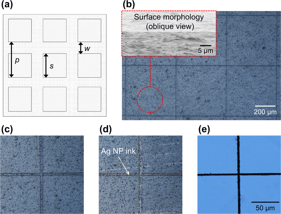
The formation of BPI-integrated metal mesh electrodes was examined through optical microscopy (OM; LV100POL, Nikon) at representative stages of imprinting, Ag NP ink filling, and selective etching, as shown in Fig. 2(b)–Fig. 2(d). After imprinting, the BPI layer showed a recessed mesh pattern transferred from the protruding PDMS stamp, with a line width of approximately 4.8 μm and a depth of approximately 900 nm (Fig. 2(b) and Fig. 2(c)). A residual BPI layer of about 200 nm remained between the recessed channel and the PEN substrate, placing the light absorption layer at the bottom of the channel where the metal mesh would subsequently be formed. After UVO treatment, the Ag NP ink was filled into the recessed channels by doctor blading, and the ink was largely confined within the patterned regions with only minor residue on the surrounding BPI surface (Fig. 2(d)). This filling behavior indicates that the surface modification of BPI helped guide the Ag NP ink into the recessed mesh channels. During the subsequent thermal treatment, the Ag NP-filled lines were sintered, while the BPI in contact with the metal mesh region underwent additional curing, thereby allowing this region to withstand the subsequent etching process. After selective etching, the optical image showed a clean metal mesh pattern with the exposed BPI regions removed (Fig. 2(e)), demonstrating that the sequential imprinting, filling, curing, and etching steps produced a metal mesh electrode integrated with a localized BPI light absorption layer.
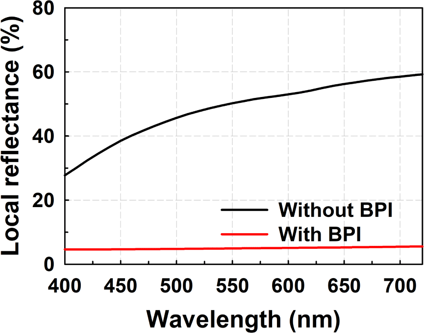
The reflectance reduction effect of the BPI light-absorption layer was evaluated by measuring the local reflectance in the Ag electrode region, where metal-induced reflection primarily occurs, using a UV–vis spectrophotometer (V-650, JASCO). At 550 nm, near the wavelength range of maximum human visual sensitivity, the Ag NP ink exhibited a reflectance of 50.22%, indicating the high apparent reflectance of the metallic electrode region. When a 200 nm-thick BPI layer was introduced beneath the Ag electrode region, the reflectance decreased to 4.94%, corresponding to a reduction of approximately 90.16% (Fig. 3). This result shows that the BPI layer absorbs reflected light from the metal region and substantially lowers the apparent reflectance of the Ag electrode. Although Ag lines occupy only a small fraction of the total area in the metal mesh electrode, they are a major source of metal-induced reflection and electrode-pattern visibility. Therefore, localizing the BPI layer beneath and near the Ag mesh lines can be considered an effective structural approach for reducing reflection from the visually dominant metal-line region without introducing a light-absorbing layer over the entire transparent area.
The characteristics of the fabricated metal mesh electrodes were evaluated in terms of sheet resistance and optical transmittance. The mesh sheet resistance measured by the Van der Pauw method was 45.6 Ω/▭, which is slightly higher than the theoretical value of 38.87 Ω/▭ estimated from the mesh resistance model [23]. This difference can be attributed to practical variations introduced during fabrication, such as deviations in line width and mesh depth, as well as incomplete filling of the recessed channels with Ag NP ink. Nevertheless, the measured sheet resistance remained below the target value of Rs,mesh<50 Ω/▭, indicating that the designed mesh geometry provided the intended electrical characteristics. In addition, the sheet resistance showed negligible change after the selective etching process, suggesting that removal of the exposed BPI regions did not significantly affect the Ag conductive network. The sheet resistance also showed negligible change after 1,000 bending cycles at a 30 mm bending radius.
The optical transmittance of the electrode film was measured using a UV–vis spectrophotometer in the wavelength range of 400–800 nm. At 550 nm, the bare PEN film exhibited a transmittance of 86.00%, whereas the metal mesh electrode film showed a transmittance of 81.92% (Fig. 4). Considering the transmittance of the PEN substrate, the normalized transmittance of the mesh structure was calculated to be approximately 95.25%, which agrees well with the design target of maintaining an open-area transmittance above 95%. The measured film transmittance was slightly lower than the theoretical value of 84.31%, likely due to residual particles or scattering centers remaining in the open regions after etching. Despite this slight optical loss, the fabricated electrode remained visibly transparent while meeting the target sheet resistance.
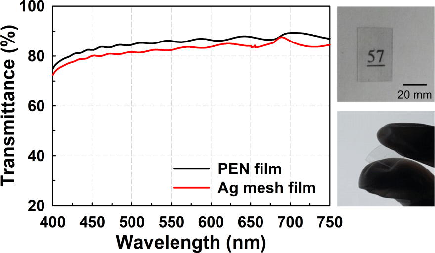
These results indicate that the fabricated electrode film satisfied the intended optical–electrical target range, while the main function of the localized BPI layer was to reduce reflection from the Ag mesh lines. The measured transmittance and sheet resistance should be interpreted together with the substrate and processing conditions used in this study, rather than as fixed limits of the proposed structure. Because the PEN substrate exhibited a transmittance of 86.00%, the total electrode-film transmittance was partly limited by the substrate, whereas the normalized transmittance of the mesh structure was approximately 95.25%. Therefore, the total transmittance could be further improved by using a substrate with higher intrinsic transparency. Similarly, the sheet resistance could be further reduced by optimizing the sintering conditions, using a higher-conductivity Ag NP ink, or increasing the mesh aspect ratio.
4. CONCLUSION
In this study, a flexible Ag metal mesh electrode integrated with a localized BPI light-absorption layer was shown to reduce metal-induced reflection. The carbon-black-dispersed PI layer was selectively retained beneath and near the Ag mesh region through thermal imprinting, Ag NP ink filling, thermal treatment, and selective etching, enabling local optical modification of the reflective metal-line region without coating the entire transparent electrode film with a light-absorbing layer. The localized BPI layer reduced the reflectance of the Ag electrode region from 50.22% to 4.94% at 550 nm, corresponding to a reduction of approximately 90.16%. Since the Ag mesh lines are the primary source of metal-induced reflection and pattern visibility, this local reduction in electrode-region reflectance offers a meaningful way to lower the apparent reflection of transparent metal mesh electrodes. The fabricated electrode satisfied the target mesh sheet resistance of Rs,mesh<50 Ω/▭ and exhibited a transmittance of 81.92% at 550 nm. In addition, the sheet resistance showed negligible change after selective etching and repeated bending, suggesting that the localized BPI integration did not substantially disturb the Ag conductive network. These results suggest that integrating a localized light- absorption layer can be a useful design approach for low-reflectance, flexible metal-mesh TCEs while preserving their basic transparent-electrode characteristics.


